
With the rapid development of electronic technology, the degree of integration and miniaturization in electronic devices are constantly improving. As a result, the problem of the space electromagnetic environment is getting more attention [1]-[2]. For this issue, the shielding cavity is often used to carry out electromagnetic shielding. Typically, different shaped holes are used for heat dissipation to reduce electromagnetic interference within the shielding cavity. However, the existence of holes creates a coupling channel that disturbs electromagnetic wave propagation, resulting in a sharp weakening of the shielding ability of the cavity [3].
At present, some analytical methods, such as the Bethe small-hole coupling [4], the Robinson equivalent circuit [5], and the Baum–Liu–Tesche (BLT) equation [6], offer the advantage of high calculation efficiency with fewer resources demanded in the shielding effectiveness (SE) calculation of the coated porous cavity [7]. However, the field distribution in the cavity must be calculated from the electromagnetic field, making the computational process more complicated. Based on the transmission line theory, an equivalent circuit model was established to determine electromagnetic SE of metal cavities covered with medium conductivity materials [8]. The position and resonance effect on SE were calculated and analyzed in this work. Alternatively, an analytical model for SE evaluation in irregular cavities under plane wave irradiation was developed using coupled electromagnetic topology theory and the BLT equation [9]. The factors affecting the SE of cavities were explored. Nevertheless, the study on the analysis of inner coating materials in the shielding cavity is still limited in this field.
The mainstream absorbing materials coated on the inner wall of the shielding cavity mainly include graphene, silicon carbide (SiC), polytetrafluoroethylene (PTFE), and Ni/rGO composites. Graphene offers advantages such as low density, corrosion resistance, good thermal stability, high conductivity, and a simple process, making it a new type of effective electromagnetic shielding or microwave absorption material [10]. SiC has strong radiation resistance, high working intensity, high thermal conductivity, good oxidation resistance, and good chemical corrosion resistance [11]. PTFE is a high-performance coating with good corrosion resistance, temperature resistance, wear resistance, and aging resistance [12]. On the other hand, Ni/rGO composite is an electromagnetic wave absorption material that combines Ni nanoparticles with graphene [13]. As mentioned above, graphene, SiC, PTFE, and Ni/rGO are considered potential shielding materials to be studied in this research.
Due to the impedance mismatch between the absorbing material and the surrounding free space, the coupling of the electromagnetic energy can be absorbed and dissipated through conversion of heat into power when the electromagnetic wave enters the absorbing material [13]. To achieve effective absorption, two conditions must be satisfied:
- i.
When an incident electromagnetic wave enters the absorbing material from a free space, most of the wave must enter the interior of the material rather than reflect back.
- ii.
Electromagnetic waves entering the material must be effectively converted into thermal energy for power dissipation.
By employing conductive or magnetic materials to construct a shielding enclosure, electromagnetic isolation can be achieved in a specific area. It means that the electromagnetic fields inside the area can be contained without leakage, while external radiating electromagnetic fields are blocked from penetration. Maxwell's equations provide the fundamental theoretical basis for addressing electromagnetic compatibility issues, formulating the intrinsic relationships between electric fields, magnetic fields, current density, and charge density. Indeed, electromagnetic waves are dynamic manifestations of electromagnetic fields, representing periodically varying electromagnetic fields propagating through space. The oscillation directions of the electric and magnetic fields are mutually perpendicular and orthogonal to the direction of wave propagation. The expressions for electric field strength Ex and magnetic field strength Hy are expressed as follows [14]:
Combined with the law of conservation of electromagnetic field energy [16], it is deduced as
When an electromagnetic wave propagates through free space and impinges on the interface of another medium, the free space impedance Z0 is obtained from (3), as shown (4). The surface impedance ZS of the wave-absorbing material is given by (5) [17]:
The BLT equation can describe the equivalent transmission characteristics of electromagnetic waves on transmission lines, including the propagation and absorption properties when electromagnetic waves enter the cavity interior. When establishing this model, the external electric field strength is converted into an equivalent potential (voltage) based on the principle of field-circuit equivalence. If an external electromagnetic wave irradiates the cavity aperture, the tangential electric field component
To match the wave modes of the transmission line, a mode-matching integration is performed on this distributed source, yielding lumped equivalent wave sources
The voltage values at each node of the network are then obtained, completing the analysis of the shielding characteristics of the cavity. Based on the aforementioned electromagnetic energy flow relationships, the signal flow graph of the cavity model constructed is shown in Fig. 1. It demonstrates the transmission paths and energy conversion processes of electromagnetic waves within the cavity structure.
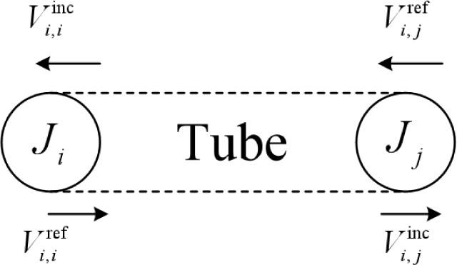
Signal flow diagram of cavity model.
Here
Results should be briefly summarized, and the authors’ main scientific contributions should be demonstrated.
In this study, the rectangular open-hole shielding cavity is taken as an example for SE analysis, and its schematic diagram is shown in Fig. 2. Here, absorbing materials are selected based on their electromagnetic parameters, such as the relative dielectric constant ɛr and relative magnetic permeability μr [13]. The rectangular hole gap has length l1 and width w1, located in the center of the front wall in the cavity. The direction of the interference electromagnetic wave electric field is along the y axis, and the propagation direction is along the −z axis, that is, vertical incidence and vertical polarization. The distance between the observation point P2 and the aperture center is d2. The distance between the observation point P1 and the aperture center is d1; the SE of the rectangular shielding cavity is obtained by calculating the voltage at the observation point P1.
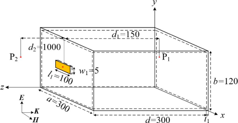
Schematic diagram of rectangular cavity model structure (unit: mm).
The schematic diagram of a cavity coated with and without absorbing material is shown in Fig. 3, where the gray area indicates no absorbing material coated, and the blue area shows the inner wall of the cavity coated with absorbing material.
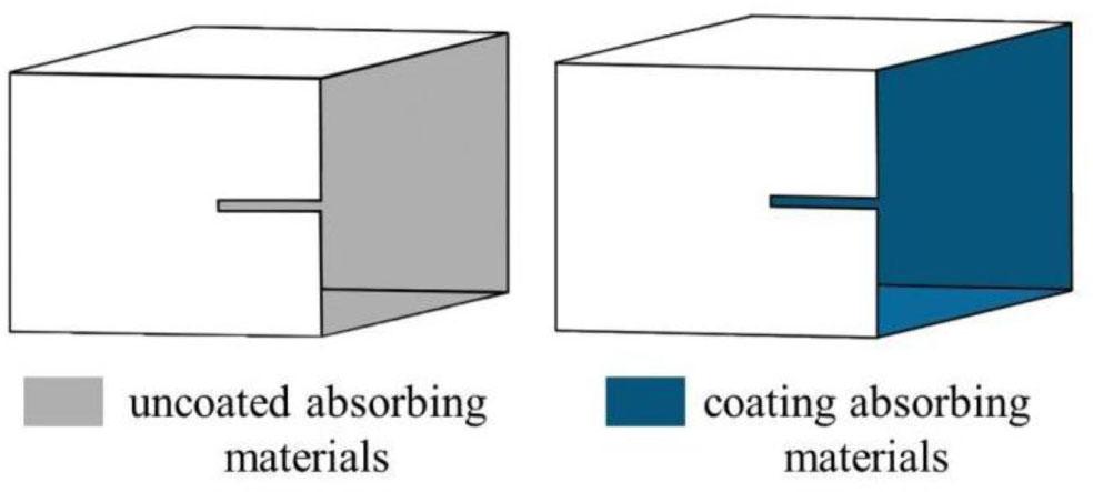
Coating schematic diagram in rectangular shielding cavities with openings.
When coating absorbing materials on the inner wall of the cavity and establishing the equivalent circuit, the aperture impedance is equivalent to Zap, which can be expressed as the parallel connection of Zap1 and Zap2. The equivalent impedance of the aperture is Zap1 (Zap1 = 1/Yap1). When using coated absorbing materials, the equivalent impedance of the absorbing material at the aperture is Zap2 (Zap2 = 1/Yap2). Zgmn1 is the characteristic impedance of the rectangular cavity, and Zgmn2 is the characteristic impedance of the coated absorbing material waveguide. The impedance at the inner wall of the rectangular cavity is equivalent to the parallel connection of Zgmn1 and Zgmn2. The equivalent circuit of anti-interference using the coating material against electromagnetic wave irradiation is therefore established, as shown in Fig. 4.
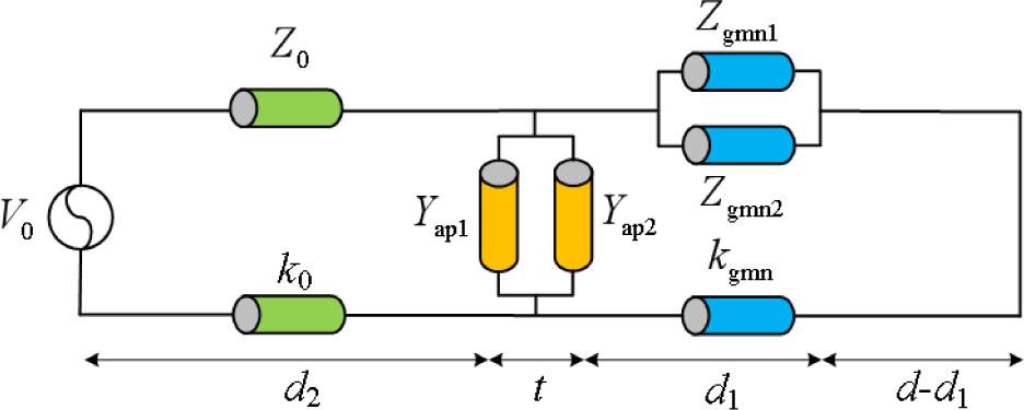
Equivalent circuit of cavity inner wall.
According to the transmission line equivalent circuit [20], voltage source V0 (V0 = 1 V) represents the external incident plane wave, and Z0 (Z0 = 377 Ω) is the characteristic impedance of free space; the external space transmission coefficient k0 = 2π/λ, where λ is the interference electromagnetic wavelength.
The equivalent impedance Zap1 of the aperture is expressed as
Zos is expressed as
The impedance and transmission coefficients in the shielding cavity are equivalent to Zgmn1 and kgmn1 in the rectangular waveguide, respectively.
In (15) and (16), the values of m and n are the number of standing waves along the x and y axes. The characteristic impedance Zgmn2 of a waveguide coated with absorbing material is expressed as
The equivalent impedance Zap of the slot in Fig. 4 is shown in (20), and the total impedance Zgmn of the rectangular waveguide is shown in (21).
According to the electromagnetic topology theory [17], the signal flow diagram of the cavity using the coated suction material is established as shown in Fig. 5. Here, Tube1 represents free space, and Tube2 and Tube3 are shielded cavity, where J1 is the cavity in vitro observation point P2, Ws is the interference electromagnetic wave equivalent voltage source, J2 is the hole seam node, J3 is the intra-cavity observation point P1, and J4 is the terminal node of the cavity.
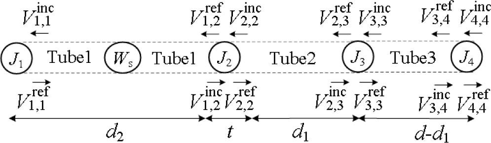
Signal-flow graph of cavity coated with absorbing material.
The BLT equation, formed from the inner wall using a coated absorbing material cavity, is established based on Fig. 4 and Fig. 5. The scattering matrix S can be obtained from the impedance, S = diag [ρ1ρ2ρ3ρ4]. ρ1 indicates the node J1 dissipation coefficient, and ρ1 = 0, ρ4 is the node J4 dissipation coefficient, and ρ4 = −1. ρi (i = 2,3,4) represents the node Jj of the scattering matrix, expressed by (22).
The transmission coefficient comprises the free-space transmission coefficient k0 and the transmission coefficient kg after the cavity is coated with an absorbing material. The transmission matrix P can be derived from the transmission coefficient, P = diag [T1T2T3], where Ti (i = 1,2,3) is the transmission matrix of each segment transmission channel, as expressed in (23).
Substitute the scattering matrix S (19) and the transmission matrix P (20) into (10) to obtain the total voltage V3,3 at observation point P1, and thus obtain the SE of the cavity, as shown in (24).
Therefore, the basic process flow diagram of the BLT equation modeling principle for the SE of the cavity coated with absorbing materials on the inner wall is shown in Fig. 6.
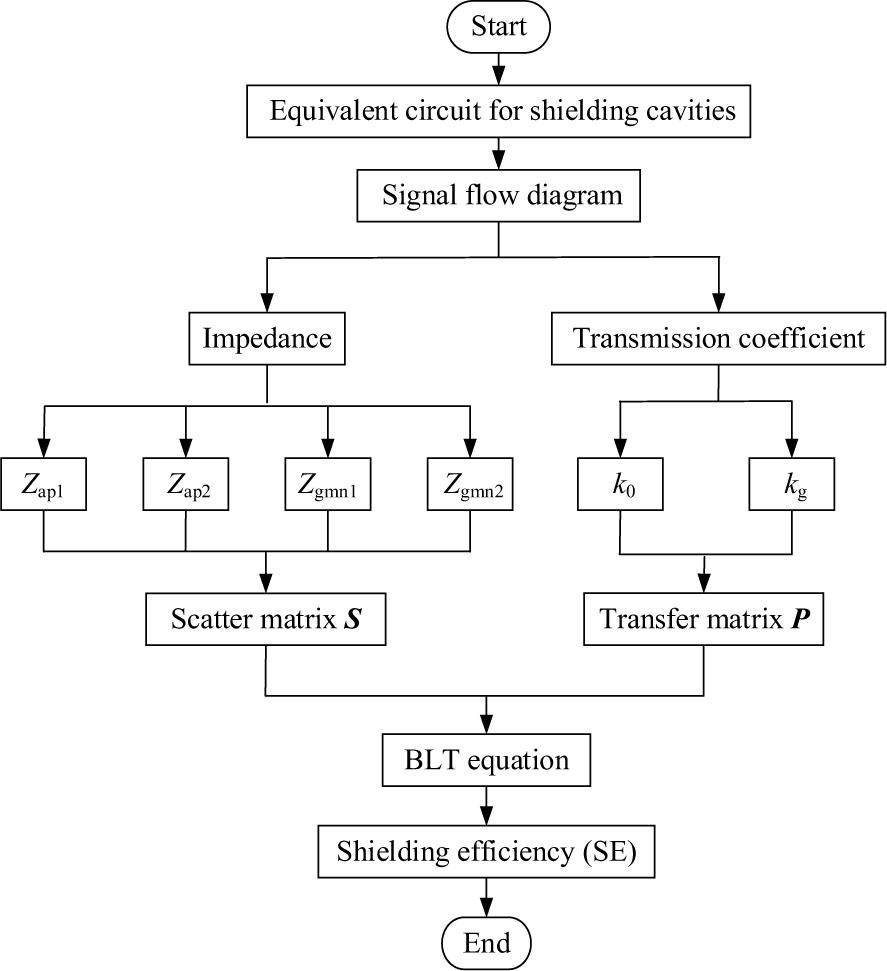
Flowchart of BLT equation modeling.
Taking the shielding cavity model shown in Fig. 2 as an example, this paper examines the effectiveness of the BLT equation topology using four absorbing materials: graphene [20], SiC [22], PTFE, and Ni/rGO composite materials [23]. The electromagnetic parameters of the absorbing material are shown in Table 1.
Electromagnetic parameters in absorbing materials.
| Material | Relative permittivity ɛr | Relative permeability μr |
|---|---|---|
| Graphene | 4.5 | 1.01 |
| SiC | 4.1 | 0.64 |
| PTFE | 2.01 | 0.95 |
| Ni/rGO | 13.45 | 1.14 |
The cavity resonance frequency fmnp is derived from the wave equation. The cavity resonance frequency is expressed in (25)
Set the frequency step Δf = 0.001 GHz at a range of 0–2 GHz with 2000 sampling points q. The calculation results from the BLT equation and CST are depicted as rBLT and rCST, respectively. The error (Δ) between rBLT and rCST is defined in (26). The average error (Δ̅) between the BLT equation and the CST simulation is shown in (27).
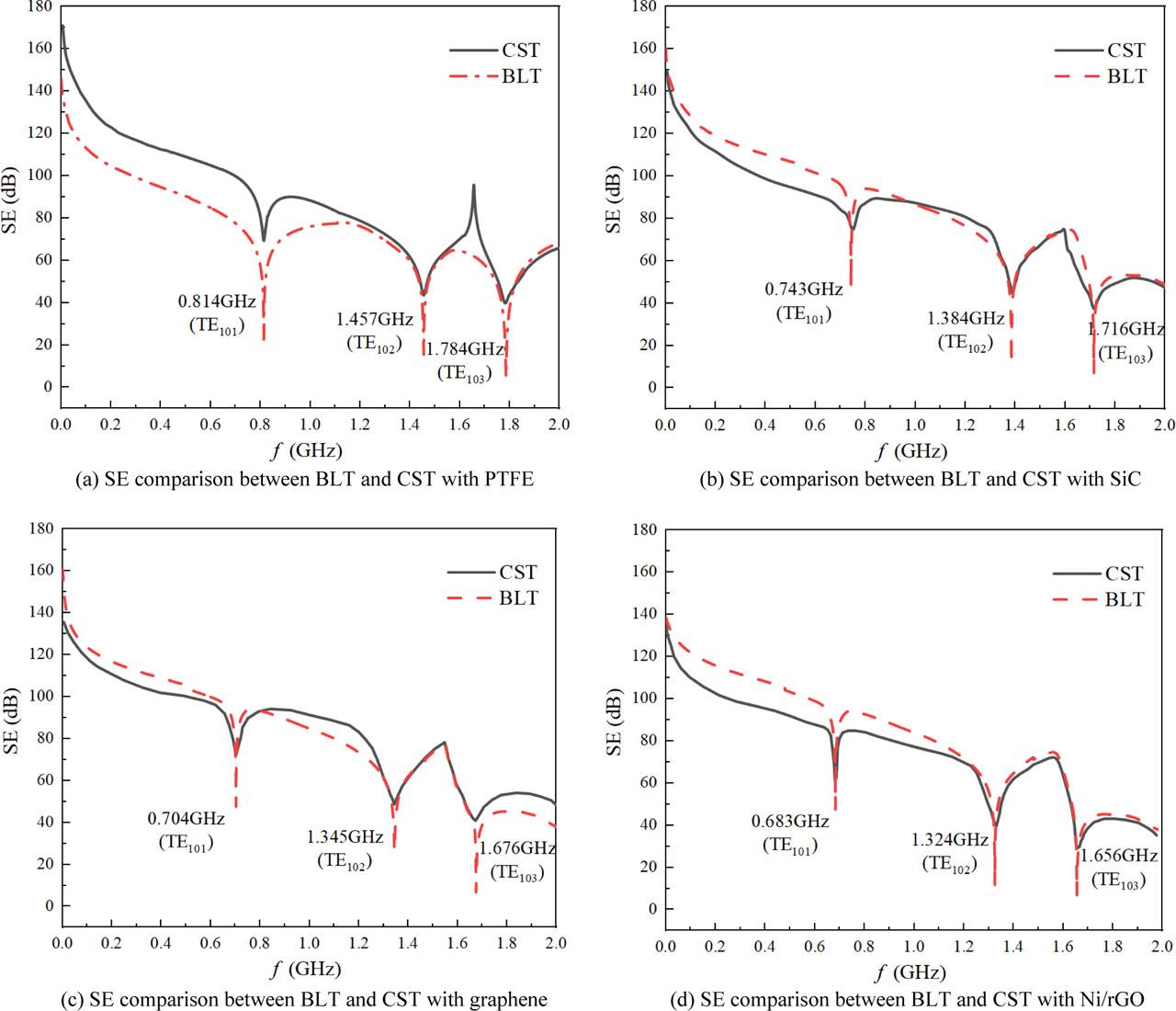
The hardware system used to implement the proposed model and CST software was an Intel i5-1135G7 2.4 GHz CPU and 16 GB memory workstation. Among four different materials, the comparison of SE vs frequency between the BLT equation and CST is shown in Fig. 7. The error (Δ) curve is shown in Fig. 8.
SE comparison in various materials.
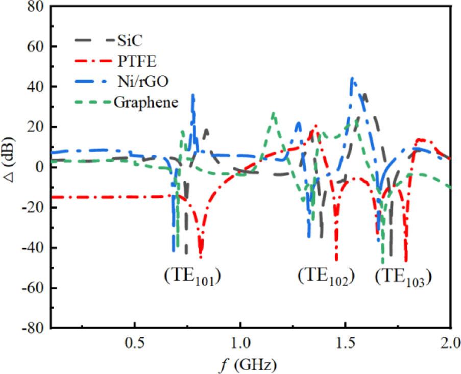
BLT equations and CST error curves for four materials.
From Fig. 7, it can be seen that the BLT equation accurately predicts the resonant frequency of the cavity in TE101, TE102, and TE103 modes. In the 0–2 GHz range, all resonant frequencies of the cavity by the BLT equation are consistent with the ones of the CST simulation results.
From Fig. 8, it is evident that SiC, PTFE, graphene, and Ni/rGO exhibit low error (Δ) between BLT and CST at all frequencies except the resonant frequency, i.e., in TE101, TE102, and TE103. This phenomenon arises due to slot resonance, where the slot size of 100 mm equals half the wavelength of the incident wave at 1 GHz. Additionally, the voltage at the resonant frequency by BLT is relatively higher than that by CST, resulting in a lower SE value.
Leveraging its equivalent circuit model based on the transmission line theory, the BLT equation requires only 2 % CPU utilization and 0.1 min to complete full-frequency band scanning, whereas CST's finite difference method, as a full-wave three-dimensional numerical simulation, demands 73 % CPU resources and 43 min. This efficiency difference is directly reflected in resonant characteristic analysis.
Although both methods yield highly consistent predictions for resonant frequencies, such as TE101 and TE102, as shown in Fig. 7, the BLT equation exhibits approximately 8 dB errors in SE calculations at resonant points (as seen in Fig. 8) due to model simplification, and therefore cannot provide a detailed internal field distribution of the cavity. In contrast, despite the longer computation time, CST can precisely quantify SE at resonant points and completely present three-dimensional field distributions, particularly demonstrating an accurate analytical capability for physical mechanisms of higher-order modes, such as TE103, affected by absorbing material thickness.
The average error (Δ̅) between BLT and CST in the four materials is summarized in Table 2, not exceeding 8 dB. It verifies the effectiveness of the BLT method in the SE of rectangular cavities coated with absorbing materials on the inner wall.
Average error in different materials.
| Material | SiC | PTFE | Graphene | Ni/rGO |
|---|---|---|---|---|
| Δ̅ [dB] | 6.01 | 7.16 | 6.68 | 7.33 |
The comparison of the average CPU utilization rate and the mean calculation time between analysis methods is shown in Table 3. It shows that the proposed model has a significantly lower average CPU utilization rate, i.e., 2 %, compared to CST software, i.e., 73 %. In the mean calculation time, the proposed model takes only 0.1 min, which is much shorter than the 43 min required by the CST software. It reveals that the proposed model can provide both fast and effective analysis in the exploration of the thickness related to the cavity shielding capability.
Comparison of average CPU utilization rate and computational time.
| Computational method | Average CPU utilization rate [%] | Mean calculation time [min] |
|---|---|---|
| The proposed model | 2 | 0.1 |
| CST software | 73 | 43 |
The resonant frequency of the cavity with various thicknesses of absorbing materials under resonant modes TE101, TE102, and TE103 is explored in this study. According to the electronic industry standard rubber-based wave absorbing plate specification SJ 21488-2018 [25], the thickness of the wave absorbing material was selected as 0.5 mm, 1 mm, 1.5 mm, 2 mm, 2.5 mm, and 3 mm.
The SE comparison in porous cavity coating at 0–2 GHz for four materials is shown in Fig. 9. It is observed that Ni/rGO exhibits the strongest electromagnetic shielding capability, while PTFE has the least effective shielding. It implies that Ni/rGO can convert incident electromagnetic waves into thermal energy more efficiently, allowing it to be dissipated via the dielectric.
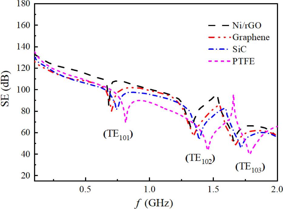
SE in different absorbing materials.
The effect of coated thickness on various materials, especially in locations with higher resonant frequencies, is shown in Fig. 10. For graphene, it is observed that the resonant frequencies in the TE101 and TE102 resonant modes correspond to 0.704 GHz and 1.345 GHz, respectively, as shown in Fig. 10(a). However, at the high-order resonant TE103, the resonant frequencies decrease with an increase in the material thickness.
The 3 mm thickness corresponds to 1.641 GHz,
the 2.5 mm thickness corresponds to 1.649 GHz,
the 2 mm thickness corresponds to 1.677 GHz,
the 1.5 mm thickness corresponds to 1.663 GHz,
the 1 mm thickness corresponds to 1.661-1 GHz, and
the 0.5 mm thickness corresponds to 1.667 GHz.
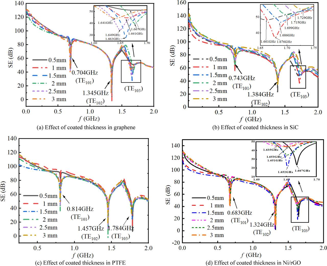
Effect of coated thickness in various materials.
It shows that the change of absorbing material thickness may affect the location of the high resonance. Through equations (10) – (20), it is revealed that the material thickness can influence the real and imaginary parts of electromagnetic parameters in the complex frequency domain. In practice, the electromagnetic parameters of graphene can be measured using the coaxial method in the frequency range of 1–18 GHz [26]. In reality, due to the weak magnetic properties of graphene materials, the real part of the complex permeability is 1, and the imaginary part is 0. As a result, only the complex dielectric constant is considered here. According to (22), the resonant frequency increases as the complex dielectric constant decreases.
As shown in Fig. 10(b), when the cavity is coated with SiC, the resonant frequencies for modes TE101 and TE102 are 0.743 GHz and 1.384 GHz, respectively, where the thickness of the coating does not change the resonant frequencies. However, the thickness has a significant influence on the frequency at the resonant mode TE103. For example, a coating of 0.5 mm thickness corresponds to 1.661 GHz, a coating of 1 mm thickness to 1.676 GHz, a coating of 1.5 mm thickness to 1.686 GHz, a coating of 2 mm thickness to 1.699 GHz, a coating of 2.5 mm thickness to 1.715 GHz, and a coating of 3 mm thickness to 1.729 GHz. The real and imaginary parts of the complex permittivity in SiC remain almost unchanged with increasing frequency, while the real part of the complex permeability decreases with increasing frequency [11]. Similar to graphene, the resonant frequency in SiC increases along with a decrease in the complex dielectric constant. Also, it reveals that the material thickness influences the location of higher resonant frequencies.
In Fig. 10(c), resonant frequencies correspond to 0.814 GHz, 1.457 GHz, and 1.784 GHz at modes TE101, TE102, and TE103, respectively, when the cavity is coated with PTFE. It reveals that the coating thickness does not influence the resonant frequency, while the thickness of PTFE can affect the SE. Indeed, the complex dielectric constant and complex magnetic permeability in PTFE do not vary with frequency. It implies that the thickness of PTFE material may not change the resonant frequency [12].
In Fig. 10(d), when the cavity is coated with Ni/rGO, the thickness has little influence on the resonant frequency in the TE101 and TE102 modes. However, in mode TE103, the thickness has a significant influence on the resonance at the higher-order frequency. For instance, the coating with a thickness of 0.5 mm corresponds to a resonant frequency of 1.667 GHz, while 1 mm and 3 mm thicknesses correspond to 1.653 GHz, 1.5 mm thickness to 1.652 GHz, 2 mm thickness to 1.635 GHz, and 2.5 mm thickness to 1.651 GHz. Therefore, the change of Ni/rGO thickness can affect the higher-order resonant frequency at TE103. It is noted that the material thickness can affect the real and imaginary parts of electromagnetic parameters. On the other hand, the real and imaginary parts of the complex permittivity in Ni/rGO remain almost unchanged with increasing frequency. However, the real part of the complex permeability decreases with increasing frequency [13].
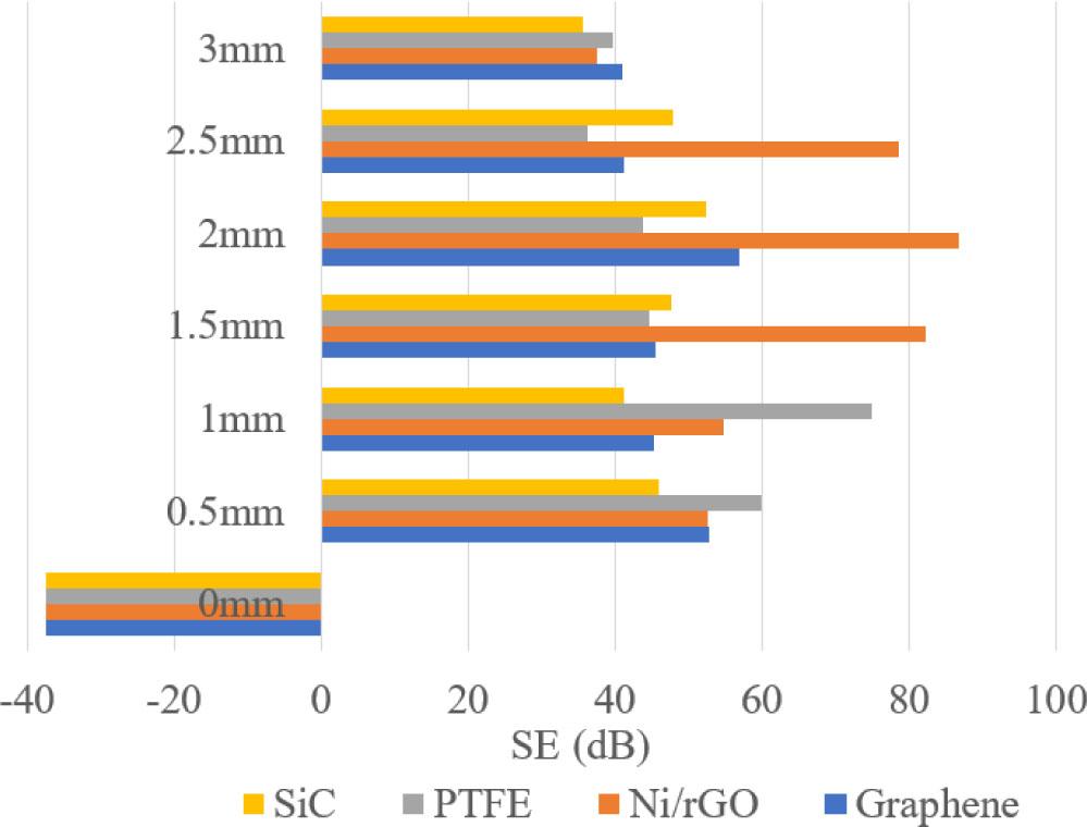
The SE comparison of absorbent materials with different thicknesses is shown in Fig. 11, indicating the SE related to the coated thickness in all materials. We observe that the cavity shielding performance achieves its best efficacy when the thickness of graphene is 2 mm, with an SE value of 56.98 dB. When the thickness of SiC is 2 mm, the SE is the best with an SE value of 86.84 dB; when the thickness of PTFE material is 1 mm, the SE is the largest with an SE value of 74.95 dB. When the thickness of Ni/rGO is 2 mm, the SE is optimal with an SE value of 52.38 dB.
Comparison of SE with different thicknesses.
In this study, the BLT-based equation analytical model has been successfully established to accurately calculate the SE of absorbing materials. It verifies that the results obtained using the BLT equation and CST simulation are very close, with an error of less than 8 dB. More importantly, the BLT equation model calculates the SE and resonant frequency more quickly than CST. In conclusion, the BLT equation can rapidly complete single SE calculations, enabling quick optimization of multiple variables, such as material thickness and dielectric parameters. This makes it particularly suitable for preliminary rapid parameter scanning and resonant risk assessment. While CST simulations are more time-consuming, they can accurately capture the field distribution characteristics of higher-order resonant modes, such as TE103, providing critical evidence for understanding electromagnetic energy coupling paths and an effective means for final design validation and mechanism investigation.
It also confirms that the inner wall of the cavity, coated with a graphene, SiC, and Ni/rGO composite material, has no effect on the frequency at the TE101 and TE102 resonant modes; however, an effect occurs at the higher-order resonant TE103 modes. However, the coated thickness using PTFE does not change the resonant frequency of the cavity. Moreover, the 2 mm thickness of the cavity wall coated with graphene, SiC, or Ni/rGO composite materials is found to achieve the best electromagnetic shielding performance. On the other hand, a 1 mm thick coating using PTFE can achieve the best SE in the cavity wall.