
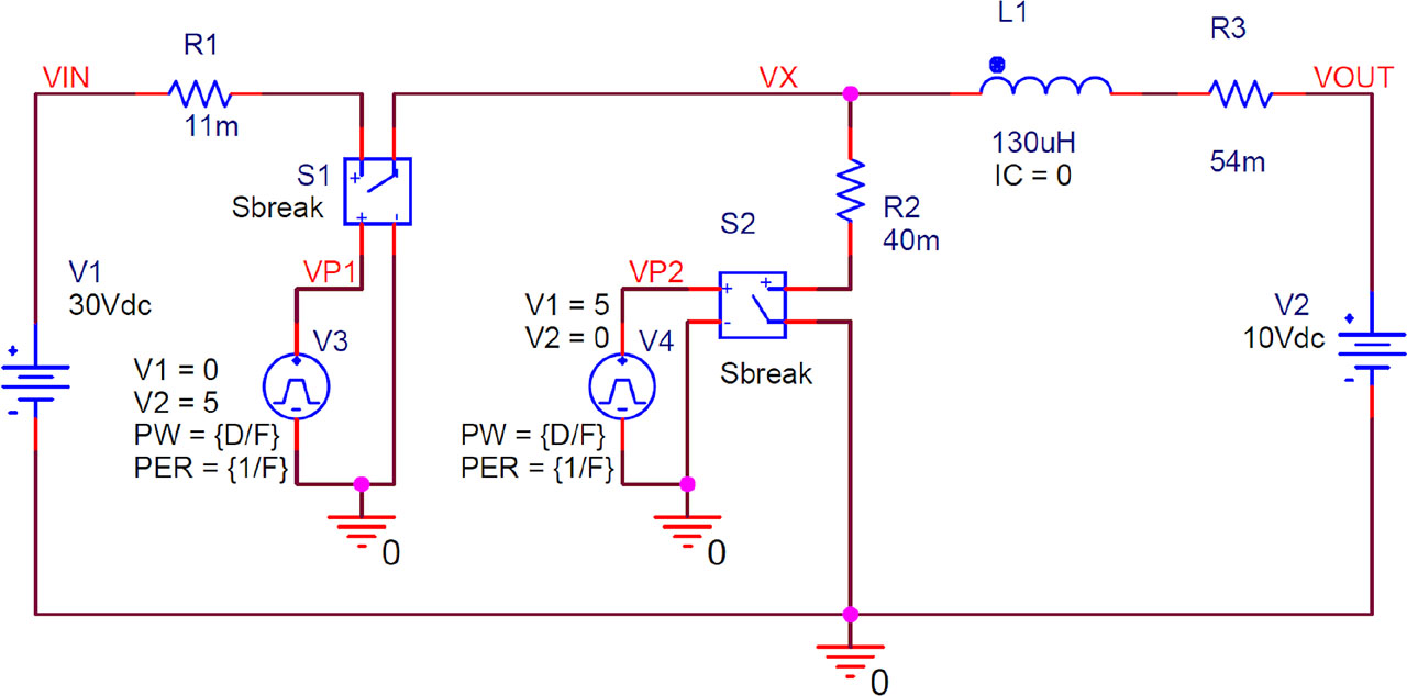
Figure 1.
Basic model for evaluating the OL converter. The parameter used is the duty cycle D, while the frequency F is fixed to 20 kHz. OL, open-loop.
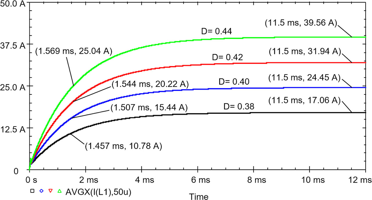
Figure 2.
PSpice simulation results of the transient response of the buck basic model working in CCM. CCM, continuous current mode.
Table 1.
Simulation results of the basic model for the OL converter.
| ISC | τ | ||||||
|---|---|---|---|---|---|---|---|
| ΔV (V) | D | Ideal (A) | Sim. (A) | Error (%) | Ideal (ms) | Sim (ms) | Error (%) |
| 20 | 0.38 | 16.87 | 17.06 | 1.1 | 1.57 | 1.46 | 7.0 |
| 0.40 | 24.27 | 24.45 | 0.7 | 1.58 | 1.51 | 4.5 | |
| 0.42 | 31.78 | 31.94 | 0.5 | 1.59 | 1.54 | 2.8 | |
| 0.44 | 39.39 | 39.56 | 0.4 | 1.60 | 1.57 | 1.9 | |
| 10 | 0.71 | 17.71 | 17.92 | 1.2 | 1.77 | 1.68 | 5.2 |
| 0.73 | 26.09 | 26.29 | 0.8 | 1.78 | 1.72 | 3.6 | |
| 0.75 | 34.60 | 34.79 | 0.5 | 1.80 | 1.76 | 2.4 | |
| 0.77 | 43.25 | 43.43 | 0.4 | 1.81 | 1.79 | 1.3 | |
| 5 | 0.85 | 7.21 | 7.44 | 3.2 | 1.87 | 1.72 | 8.2 |
| 0.87 | 16.00 | 16.22 | 1.4 | 1.89 | 1.82 | 3.7 | |
| 0.89 | 24.93 | 25.14 | 0.8 | 1.91 | 1.88 | 1.4 | |
| 0.91 | 34.02 | 34.22 | 0.6 | 1.92 | 1.91 | 0.7 | |
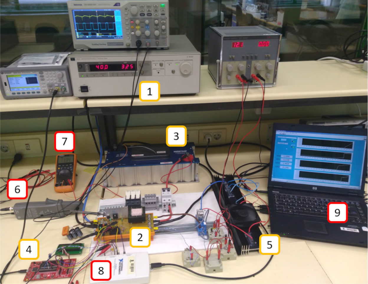
Figure 3.
Picture of the charger and test setup. (1) Input power supply. (2) Main board. (3) SC module. (4) 8-bit μC board. (5) Resistive load. (6) Input current probe. (7) SC voltage tester. (8) DAQ. (9) Data-logging and monitoring virtual instrument. DAQ, data acquisition system; SCs, supercapacitors.
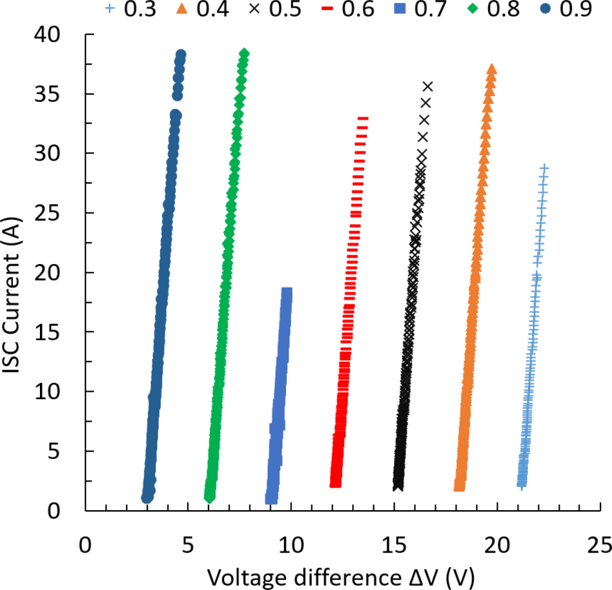
Figure 4.
Output charging current versus the voltage difference variations (ΔV) for several duty cycles.
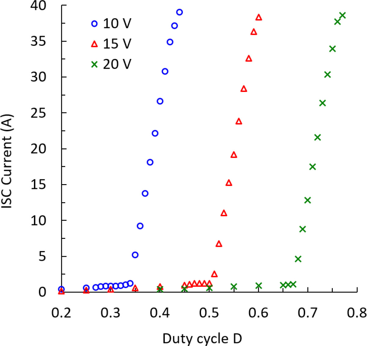
Figure 5.
Output charging current versus the duty-cycle variations for 30 V at the input and several initial voltages across the SCs (10 V, 15 V and 20 V). SCs, supercapacitors.
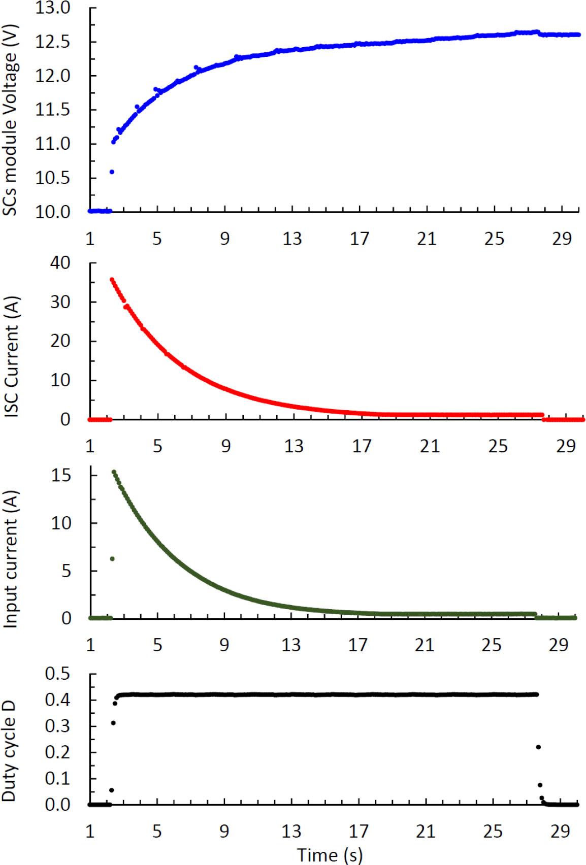
Figure 6.
Variables evolution for a charging process for 30 V input voltage and 10 V initial output voltage across the SCs, and a duty cycle of 0.42. SCs, supercapacitors.
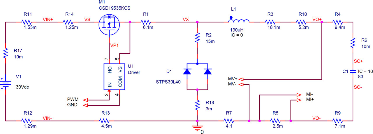
Figure 7.
Schematic of the realistic model with fitted parameters. The MV signal is connected to a voltage divider to get a value ranging between 0 V and 5 V. The MI signal is connected to a differential amplifier 25-gain followed by a low-pass filter. Finally, both are connected to a two-channel ADC that sends the measurements to the μC via an SPI connection. ADC, analog-to-digital converter; MI, measuring intensity; MV, measuring voltage; SPI, serial port interface.
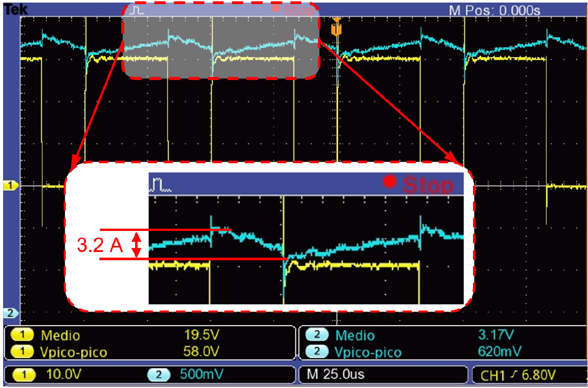
Figure 8.
Waveforms of the voltage VX at the switch output and of the load current.
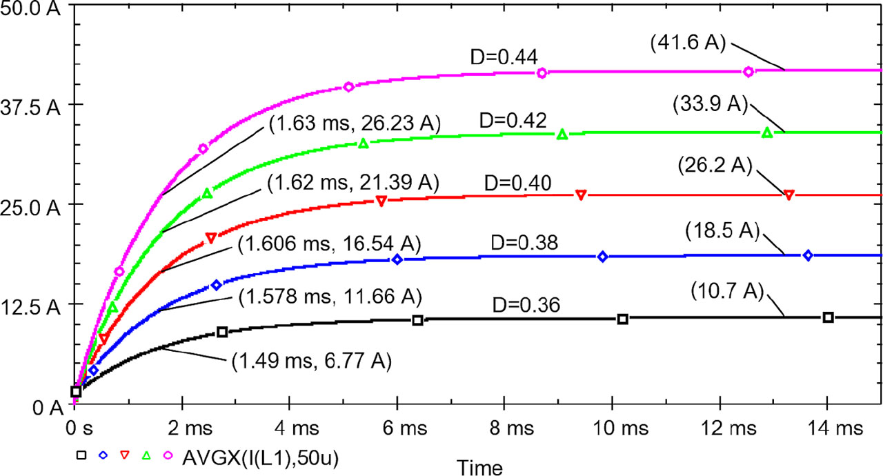
Figure 9.
Transient in load current (average) for different values of duty cycle D having VIN = 30 V and VOUT = 10 V (ΔV = 20 V).
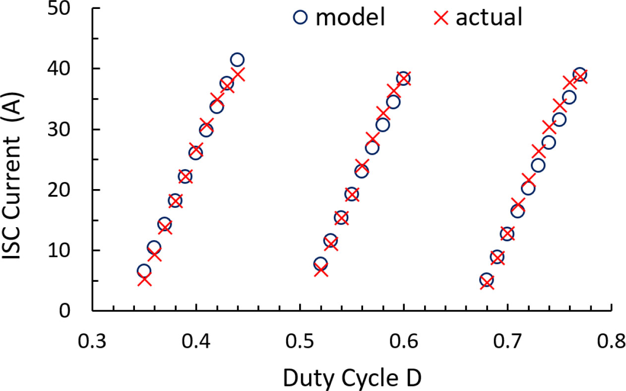
Figure 10.
Charging currents through the SCs for an input voltage of 30 V and different duty cycle values and output voltages across the SCs (from left to right: 10 V, 15 V and 20 V). Notice that these tests achieve the limit of the current measurement range. Therefore, a slight effect of saturation is observed. SCs, supercapacitors.
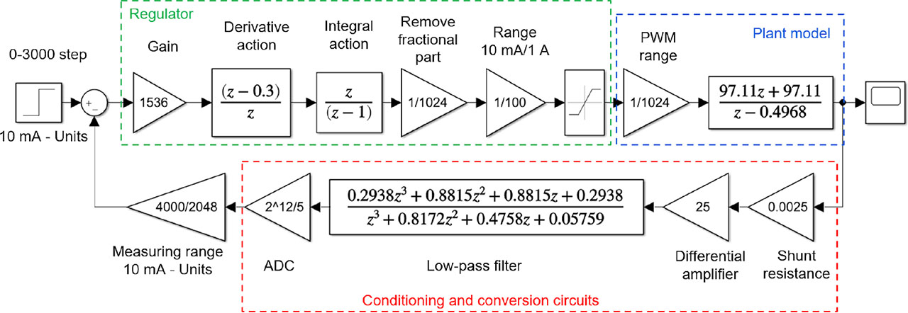
Figure 11.
CL model of the complete system. CL, closed-loop.
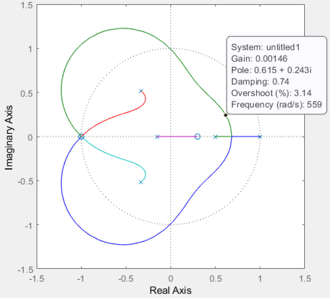
Figure 12.
Root locus of the complete system.
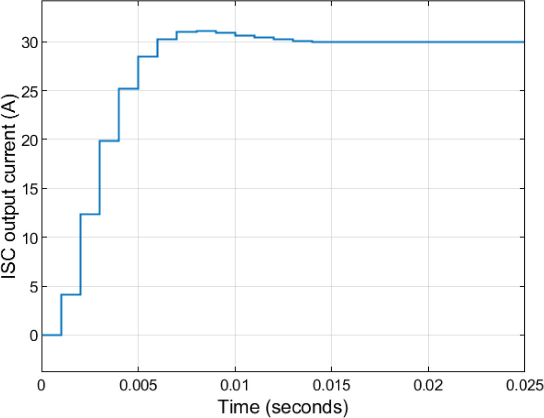
Figure 13.
Transient response to an input step of 30 A.
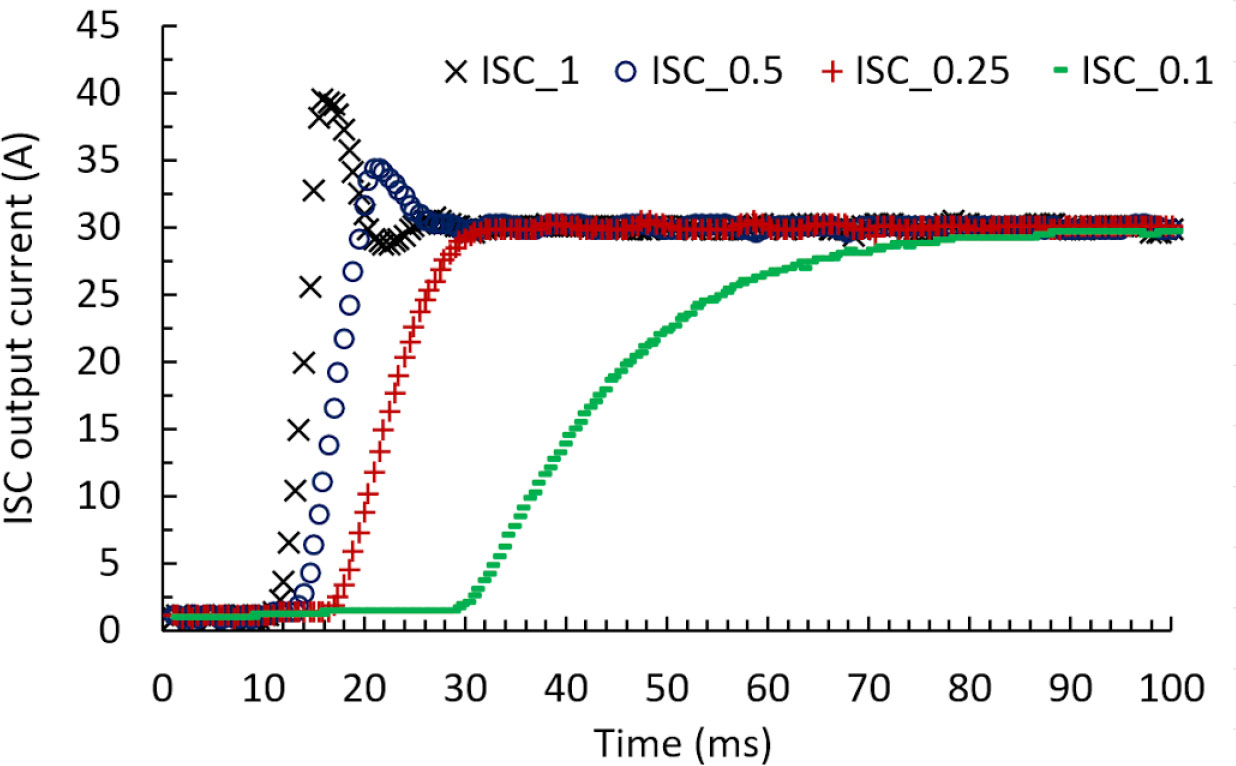
Figure 14.
CL transient response to 30 A steps for different gains. CL, closed-loop.
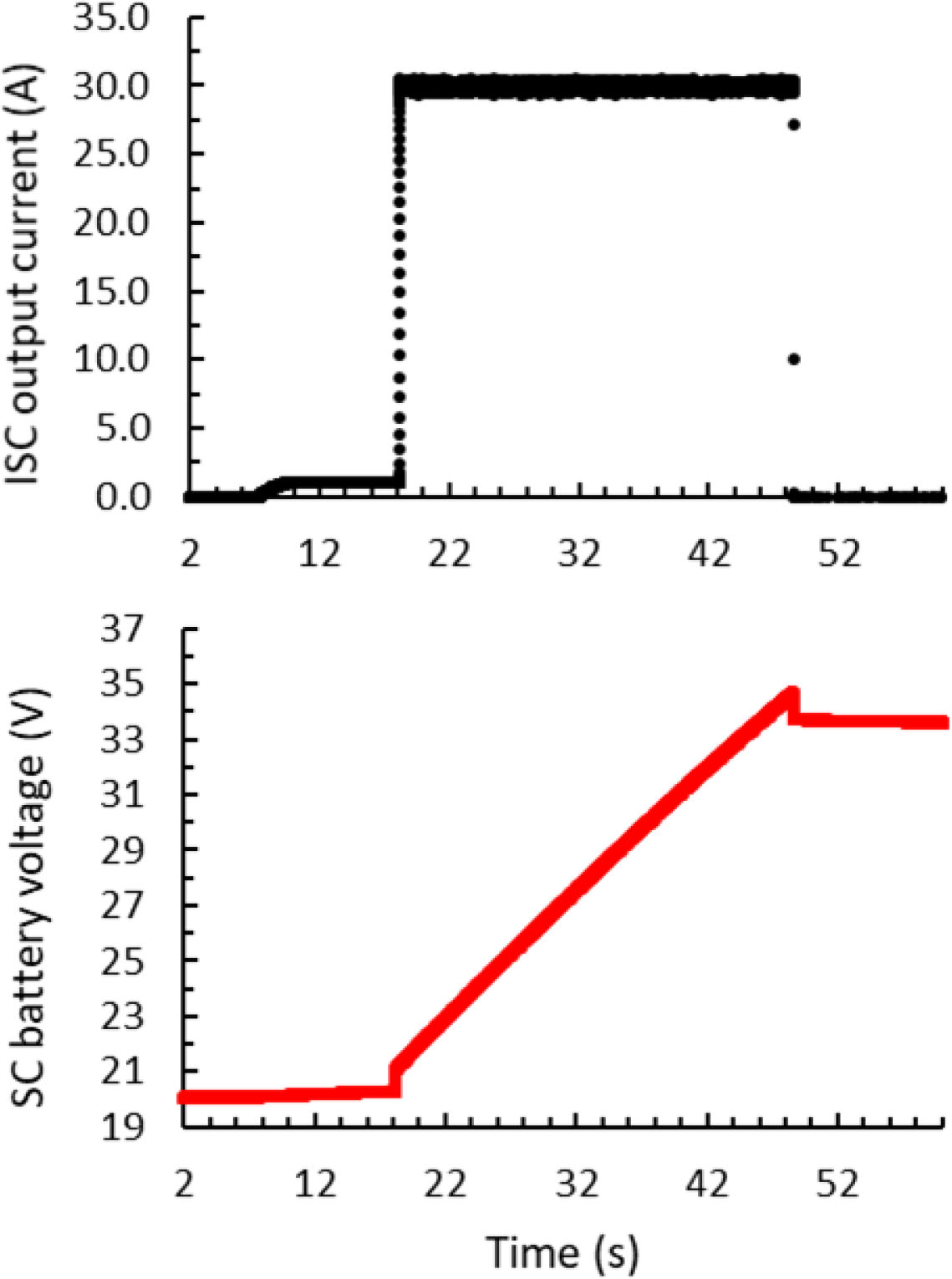
Figure 15.
Response to a step from 1 A to 30 A with a gain of 384. SC, supercapacitor.
Table 2.
Step response for different bibliographic references.
| Reference | Step size (A) | Time response (s) | Slope (A/s) |
|---|---|---|---|
| Chen, et al. (2016) | 1 | 0.054 | 18.5 |
| Rigogiannis et al. (2018) | 2.5 | 0.043 | 58 |
| Yang et al. (2019) | 500 | 0.470 | 1,000 |
| Guerriero et al. (2020) | 120 | 0.100 | 1,200 |
| Wang et al. (2021) | 22 | 0.100 | 220 |
| This work | 30 | 0.015 | 2,000 |