
Supercapacitors (SCs) have a high power density if they are compared to other energy storage technologies, since they exhibit a very low internal resistance (IEC, 2006; Morandi et al., 2021; Quintáns et al., 2017). For this reason, they are effective when combined with electrochemical accumulators (Wang et al., 2022; Zhang et al., 2020), for example, Li-ion batteries, which have a high energy density despite having a greater internal resistance. These hybrid energy storage systems (HESS) can be implemented in active structures (Pirienko et al., 2016; Zhang and Li, 2020), which are generally made up of a DC bus, the two types of electrical energy accumulators, the different loads, and the suitable DC–DC converter topologies (Baïlo Camara et al., 2008; Broday et al., 2015; Hang et al., 2023; Tan et al., 2024; Vinnikov et al., 2010).
A typical structure is the so-called SC semi-active HESS (Izadi and Beiranvand, 2023, Figure 2), in which the terminals of a Li-ion accumulator constitute the main DC bus. The different loads and their respective controllers, along with the SCs (it is assumed a module composed of a set of cells connected in series), are connected to this bus. The role of SCs is to absorb or to provide the current peaks demanded by the loads, through a bidirectional converter (Sarif et al., 2018). Assuming a large SC voltage range below the DC bus voltage, the converter should operate as a current mode booster when the SCs provide power and as a buck when they absorb power. Thus, when energy must be suddenly recovered, for example from regenerative braking (Jin et al., 2023), the converter must operate as a buck to absorb these power peaks, by quickly charging the SCs. To achieve this, not only is it necessary to regulate a high current intensity, but the response time must also be fast. In addition, when no high-power transients occur, the energy stored in the SCs can be used to charge the batteries via a booster operating at a lower current, maintaining good energy efficiency and preventing a reduction in battery life. Finally, when a load demands a high peak current, the converter must work as a booster, driving current from the SCs to the bus.
Suitable models are needed to implement this semi-active HESS, both for the case of the buck and the boost converter (bidirectional). This study addresses the case of the buck converter working in continuous current mode (CCM) for efficiently charging the SCs, covering modelling, simulation, and practical implementation. Its main contribution lies in the detailed consideration of loss resistances in the model, contributing to a more accurate depiction of the converter’s behaviour in real-world scenarios and to facilitate the regulator design. The proposed model differs from those presented in the aforementioned bibliography in that, cycle by cycle of switching, it considers the voltages of the DC bus and the SCs to be constant. Therefore, small variations in the duty cycle cause large changes in the output current. This makes it imperative to consider the loss resistances of the circuit elements to effectively control the output current, in a stable, fast and simple manner.
In Section 2, the basic model of the converter is analysed by simulation, taking into account the series resistances of both the components and the connections. The expression of the final current value for the CCM working in open-loop (OL) is deduced, as well as the characteristic time constant. Section 3 presents the practical results of the assembled converter, including the digital regulator. These results validate the model and its OL operation, as well as the regulator performance in closed-loop (CL) mode. Finally, Section 4 presents the conclusions and possible extensions that can provide continuity to this work.
Figure 1 shows a simplified model of the buck made of three branches, where the resistors (R1, R2 and R3) group the loss resistances (series resistances) of all the devices and connections of each branch. The first branch consists of the input voltage V1 corresponding to the DC bus, the loss resistor R1 and the switch S1. The second branch consists of switch S2 and loss resistor R2. The third includes the coil L1, the loss resistor R3 and the SCs represented by V2. Note that, cycle by cycle of the switches, the voltages across the DC bus and the SCs are modelled by DC generators because their voltages are considered constant. This can be assumed if a distributed parameter model is taken for the SCs as in the study by Quintáns et al. (2017), and it is supposed that the branch with the lowest time constant is the one with the greatest influence on the controller’s behavior. Although the model has been validated for different resistance values, those in Figure 1 have been chosen as an example, considering that they are realistic ones.
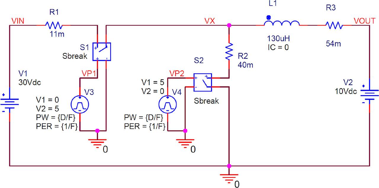
Basic model for evaluating the OL converter. The parameter used is the duty cycle D, while the frequency F is fixed to 20 kHz. OL, open-loop.
Note that, when the input voltage is constant, the buck converter can work well in CCM if the output voltage is variable. However, if both the input and output voltages are considered constant, the currents can grow strongly even if the duty cycle slightly increases, at least during a few switching periods. In this situation, the actual limit is set by the duty cycle and the equivalent series resistance (ESR) of devices and wires.
In CCM, current flows through the first and third branches when the coil is being charged and through the second and third branches when it is discharging. To simplify the analysis, it is assumed that there is a negligible current ripple and that the final steady-state average current through the coil (L1) and SCs (V2) is named ISC.
From this model, an analysis based on the principle of energy conservation can be performed, considering the average currents through the DC generators and the effective currents through the resistors. It is stated that, for a complete steady-state switching cycle, the input power provided by V1 is
If D is the duty cycle, the average input current through S1 is ISC · D, and the output current is ISC. Taking the waveforms for the currents through each branch, it is derived that the effective currents through R1, R2 and R3 are
Finally, it follows from Eq. (4) that the final output average current is given by
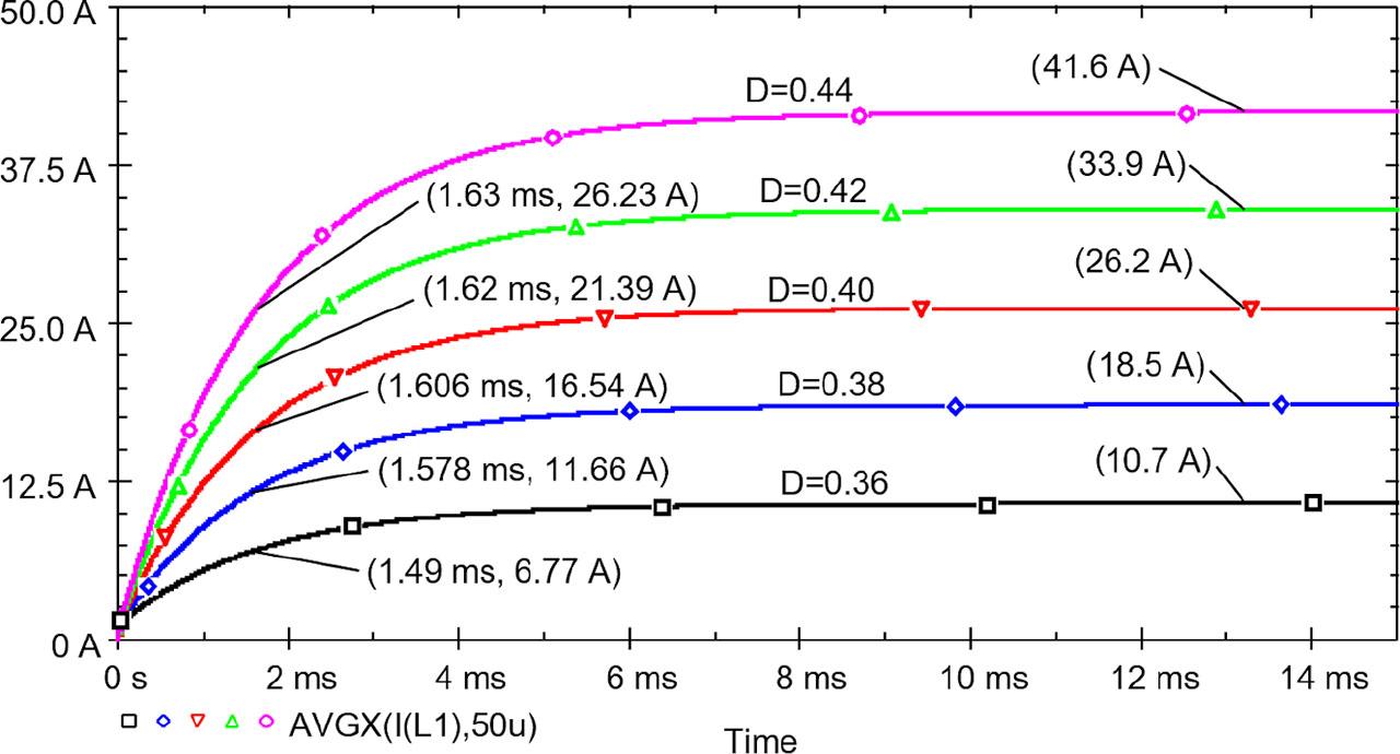
In addition to obtaining the static gain, it is necessary to evaluate the OL time constant to complete the converter model. Figure 2 shows the transient response of the output current starting from zero initial current until achieving the steady state current ISC. In this case, the graphs correspond to duty cycles D between 0.38 and 0.44 with increments of 0.02. The ratio between the increments of ISC and D gives an average static gain of 375 A/D (amperes per duty cycle). As it is a very high gain, regulation in CCM becomes difficult, and a high pulse width modulation (PWM) resolution could be necessary. As will be seen below (Subsection 3.2), this gain does not depend on the difference between the input and output voltages (∆V). On the other hand, the values of the time constant τ are taken at the 63% of ISC. In addition, it is deduced that τ and, therefore, the equivalent resistance seen by the coil depend on D.
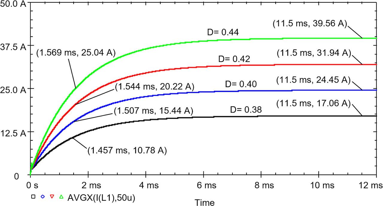
PSpice simulation results of the transient response of the buck basic model working in CCM. CCM, continuous current mode.
More simulations have been done for different duty cycles (D) and input-output voltage difference (∆V). Table 1 summarises the results for the final average current (ISC) and time constant. For each case, the ideal value (Ideal), the simulated value (Sim) and the relative error are shown. The ideal ISC value is calculated using Eq. (5), while for τ, the value of coil L1 is divided by the resistance it sees, which corresponds to the denominator of Eq. (5).
Simulation results of the basic model for the OL converter.
| ISC | τ | ||||||
|---|---|---|---|---|---|---|---|
| ΔV (V) | D | Ideal (A) | Sim. (A) | Error (%) | Ideal (ms) | Sim (ms) | Error (%) |
| 20 | 0.38 | 16.87 | 17.06 | 1.1 | 1.57 | 1.46 | 7.0 |
| 0.40 | 24.27 | 24.45 | 0.7 | 1.58 | 1.51 | 4.5 | |
| 0.42 | 31.78 | 31.94 | 0.5 | 1.59 | 1.54 | 2.8 | |
| 0.44 | 39.39 | 39.56 | 0.4 | 1.60 | 1.57 | 1.9 | |
| 10 | 0.71 | 17.71 | 17.92 | 1.2 | 1.77 | 1.68 | 5.2 |
| 0.73 | 26.09 | 26.29 | 0.8 | 1.78 | 1.72 | 3.6 | |
| 0.75 | 34.60 | 34.79 | 0.5 | 1.80 | 1.76 | 2.4 | |
| 0.77 | 43.25 | 43.43 | 0.4 | 1.81 | 1.79 | 1.3 | |
| 5 | 0.85 | 7.21 | 7.44 | 3.2 | 1.87 | 1.72 | 8.2 |
| 0.87 | 16.00 | 16.22 | 1.4 | 1.89 | 1.82 | 3.7 | |
| 0.89 | 24.93 | 25.14 | 0.8 | 1.91 | 1.88 | 1.4 | |
| 0.91 | 34.02 | 34.22 | 0.6 | 1.92 | 1.91 | 0.7 | |
Output charging current and time constant.
OL, open-loop.
As the current increases, the error in the estimation of the current and the time constant decreases. This can be attributed to the way the average current is obtained in the simulation and to the ripple effect. In general, these errors can be considered low (<10%). In the case of high currents, the error is even smaller (<1%), so that Eq. (5) can be considered valid. From these results, it can be deduced that the pole of the OL model will vary depending on the working conditions (D).
For this example, the variation of the equivalent resistance that is seen by the coil [denominator of Eq. (5)] can be estimated between 68 mΩ (D = 1) and 83 mΩ (D = 0), which implies a frequency range for the real pole between 523 rad/s and 638 rad/s (83–101 Hz). Therefore, it is concluded that the OL performance of the converter can be modelled as a first-order system with a static gain of 375 A/D and a pole at 580 ± 57 rad/s (average and variation).
This section presents the circuits and the test setup used to validate the converter model. In a scenario where electrical energy is used to power and control electromechanical systems, such as electric vehicles or elevators, response times in the order of milliseconds are required. Therefore, it is assumed that the controller of the converter does not need to operate on every switching cycle of the digital PWM. Moreover, to use a small coil, it is better to maintain a high switching frequency, in the order of tens of kilohertz. Following these criteria, a PWM configured with a frequency around 20 kHz has been used for the tests.ho.
Figure 3 presents the complete system to evaluate the charger performance, both in OL and CL (see Subsections 3.2 and 3.3). To validate the model, a converter has been built to feed a BMOD0083 P048 B01 SC module with a capacitance of 83 F (18 cells of 1,500 F in series) that can support voltages of up to 48 V (Maxwell Technologies, GmbH, 2013).
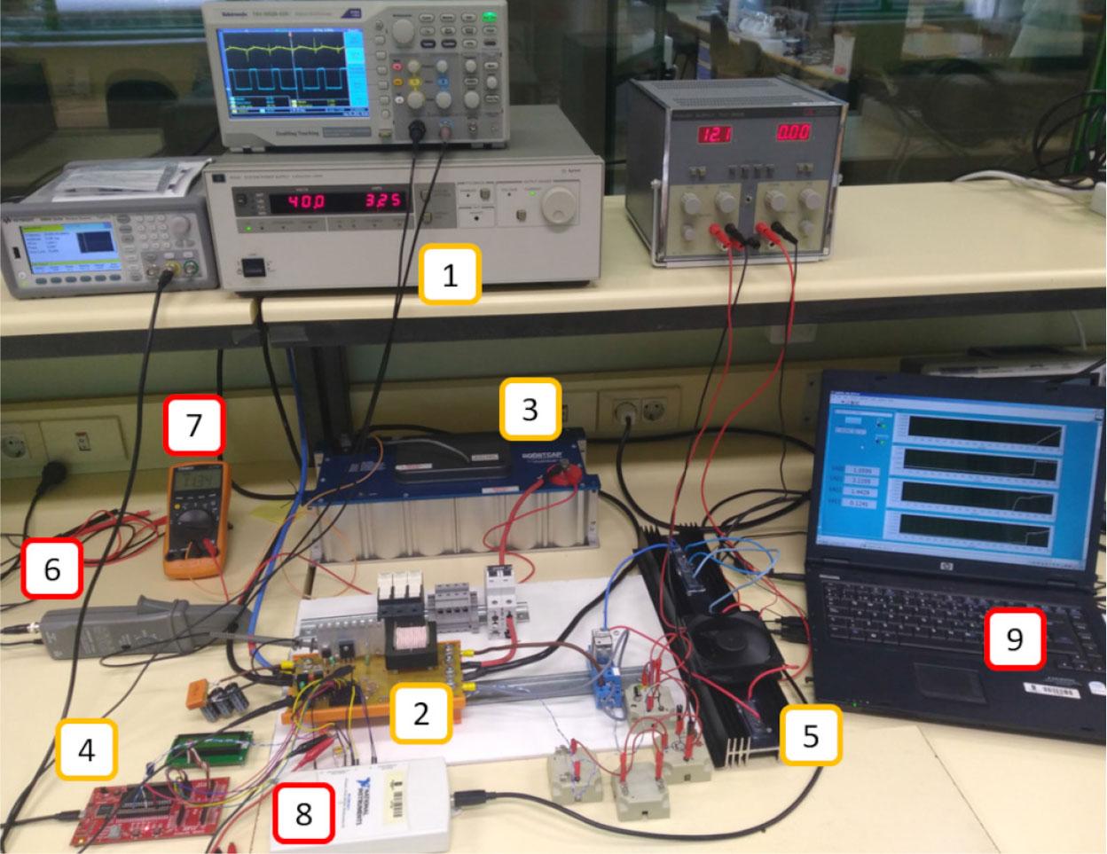
Picture of the charger and test setup. (1) Input power supply. (2) Main board. (3) SC module. (4) 8-bit μC board. (5) Resistive load. (6) Input current probe. (7) SC voltage tester. (8) DAQ. (9) Data-logging and monitoring virtual instrument. DAQ, data acquisition system; SCs, supercapacitors.
The input voltage is obtained from a 6032A power supply, which emulates the DC bus (VIN). For OL testing, a Keysight 33622A generator has been used to obtain the 20 kHz PWM signal with a good resolution (four digits). The main board contains the power devices (transistor, diode and coil), the IR2125 driver for the CSD19535KCS transistor and the conditioning circuits. The latter provides the output current and voltage levels, both in analogue and digital format via serial port interface (SPI) connection. Notice that it is assumed that knowing the voltage across the SC module is enough to determine its state of charge.
To monitor the variables, a data acquisition system (DAQ) NI-USB-6211 is used together with a virtual instrument in the computer. The output current (ISC) charging the SCs is obtained from a Shunt resistor and a differential amplifier with a gain of 25, followed by a third-order low-pass filter with a cut-off frequency of 500 Hz. The resulting output current measurement range is ±40 A.
Figure 4 represents the variation of ISC current for different duty cycles versus the difference between the input and output voltages (∆V). As expected, a high slope of ISC is reached. Taking into account the average and the typical uncertainty, a slope of 23.5 ± 0.8 A/V is obtained. This means that, for a given duty cycle, a small voltage difference results in a large current variation. Figure 5, on the contrary, shows the dependence of the ISC on D.
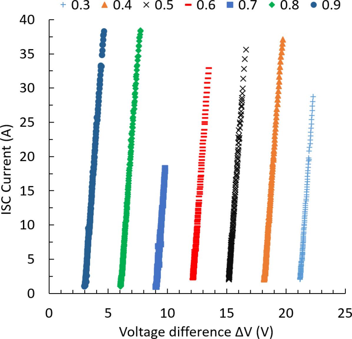
Output charging current versus the voltage difference variations (ΔV) for several duty cycles.
In contrast, Figure 5 shows the ISC dependence on D. The dots on the graph correspond to different charging tests, in which the input voltage (VIN) is fixed at 30 V and the initial voltage of the SCs is varied for each test. For example, the 10 V curve implies that for each test, the initial voltage of the SCs is always 10 V, i.e., the initial voltage difference between input and output (∆V) is 20 V. For each point on the graph, the charging process was started with a given D so that data were taken for the discontinuous current mode (DCM) and CCM operations regions.
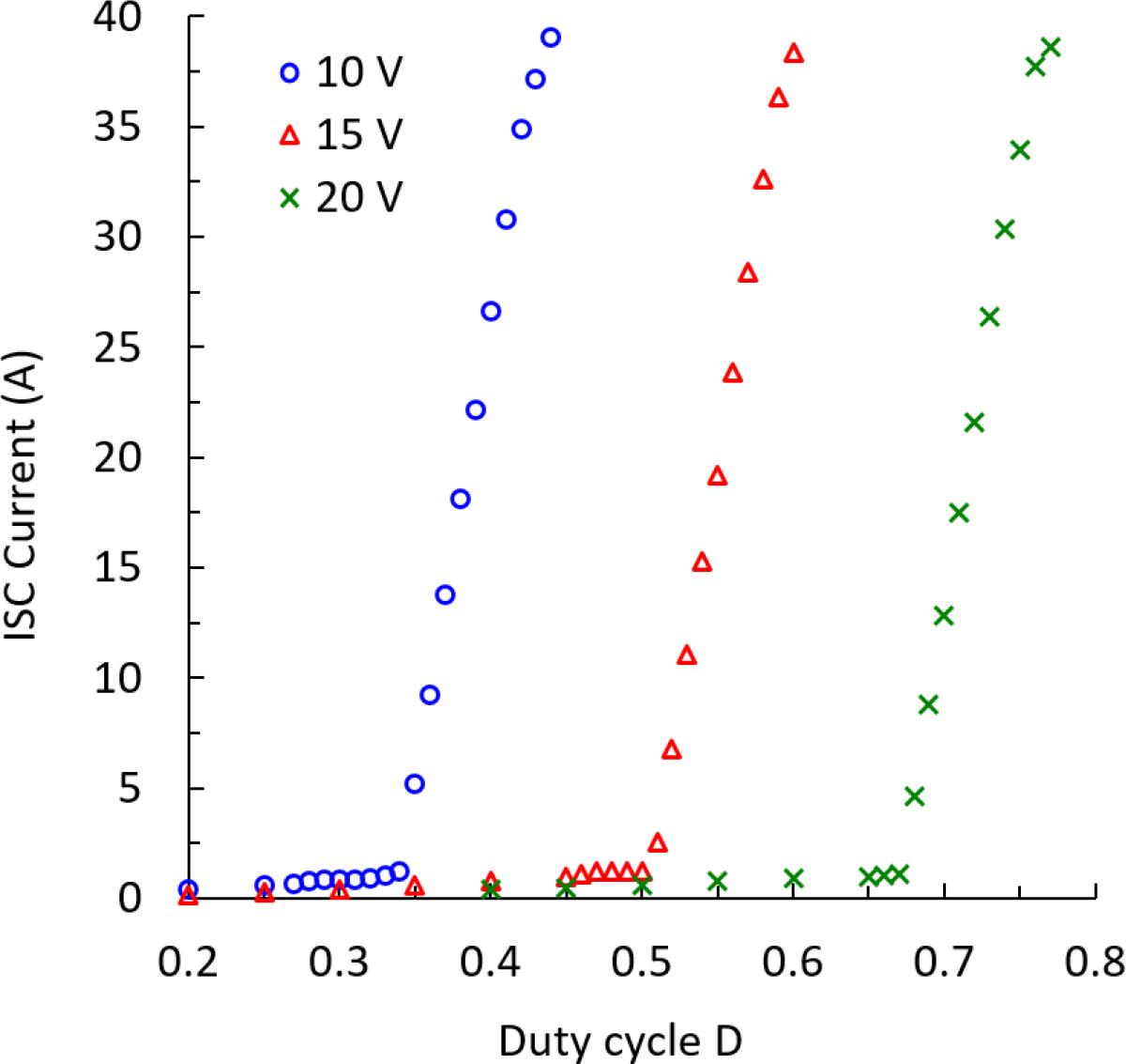
Output charging current versus the duty-cycle variations for 30 V at the input and several initial voltages across the SCs (10 V, 15 V and 20 V). SCs, supercapacitors.
It is observed how, upon entering CCM, the current increases sharply for a small variation of D. Taking the average and twice the standard deviation yields a slope of 382 ± 4 A/D. In other words, a 10% variation in D results in a variation of about 39 A at the output. In practical terms, for instance, a one-unit change in a 10-bit PWM causes a variation of 377 mA (386/1,023 mA) in the output current. Notice that the upper value of the slope (386 A/D) will be used later as the OL gain in the plant model (see Subsection 3.3). Moreover, from this analysis, it can be concluded that the ISC slope does not depend on either ∆V or D.
As an example, Figure 6 shows the beginning of the charging process for one of the dots in Figure 5. The SCs are initially charged to 10 V, and the input is set to 30 V. By activating the control pulses with a duty cycle of 0.42, charging is started with an initial current of 34.9 A, causing an instantaneous voltage increase of 1.014 V in the SCs. This implies that the equivalent resistance of the output branch is close to 29 mΩ (connections and internal resistance of the SCs). The output resistance has been calculated for all the tests in Figure 5, yielding an average value of 29 ± 5 mΩ. From the currents and voltages, it is also deduced that the initial input power is 460.74 W (15.358 A and 30 V), and the output power is 384.94 W, giving an efficiency of 83.5%, which increases as the current decreases, reaching 99% when the output current is <10 A.
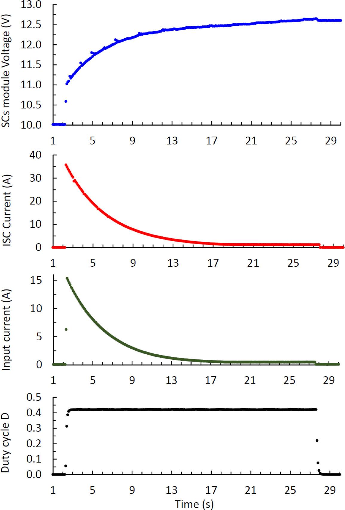
Variables evolution for a charging process for 30 V input voltage and 10 V initial output voltage across the SCs, and a duty cycle of 0.42. SCs, supercapacitors.
According to the implemented circuit, a more detailed electrical schematic of the converter model is shown in Figure 7. The resistances of the active devices (R1 for the transistor and R2 for the diode) were estimated using the information from the datasheets, as well as the ESR of the SC module (R6). The coil resistance was estimated by measuring its voltage drop when a current was injected through it. This method was also used for the cables (R11, R12, R4 and R9) and for the printed circuit board (PCB) trace sections (R14, R13, R18, R10 and R7).
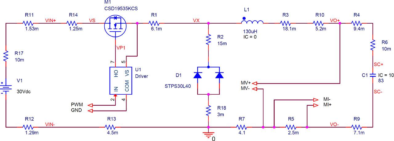
Schematic of the realistic model with fitted parameters. The MV signal is connected to a voltage divider to get a value ranging between 0 V and 5 V. The MI signal is connected to a differential amplifier 25-gain followed by a low-pass filter. Finally, both are connected to a two-channel ADC that sends the measurements to the μC via an SPI connection. ADC, analog-to-digital converter; MI, measuring intensity; MV, measuring voltage; SPI, serial port interface.
It should also be noted that the total equivalent resistance (R4 ± R6 ± R9 ± R5) at the voltage measurement points (MV±) should be 29 mΩ. This value can be deduced from the voltage increment produced when current pulses are injected (such as the example in Figure 6).
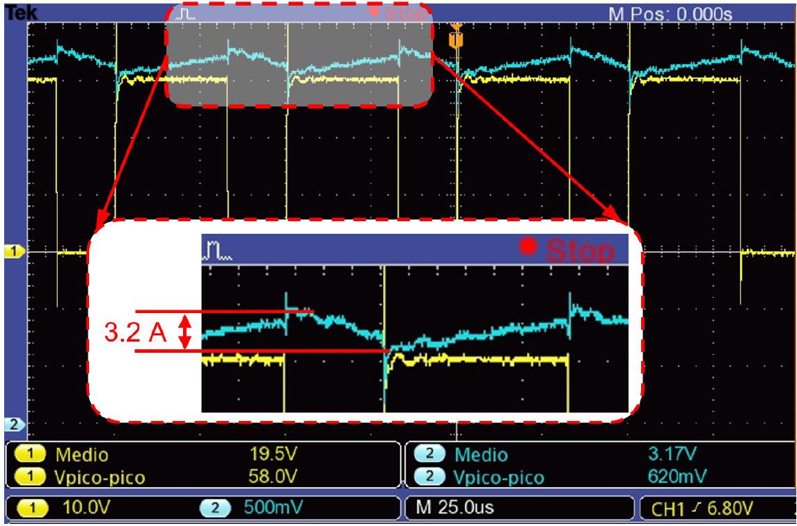
Waveforms of the voltage VX at the switch output and of the load current.
To measure the current, the voltage drop across shunt resistor R5 is amplified by a factor of 25 and filtered using a third-order low-pass filter with a cut-off frequency of 500 Hz. As the measurement circuit operates between 0 V and 5 V, a 2.5 V reference is used for the offset.
The oscillogram depicted in Figure 8 shows the voltage on node VX at the output of transistor M1 (CH1-yellow) and the waveform of the output current (CH2-blue) corresponding to a duty cycle of 0.66. The voltage signal is square, indicating that it is indeed working in CCM. The current measurement (MI) is also observed to be in CCM, with an average value of MI = 3.17 V. According to Eq. (6), this implies that the load current is 10.7 A, since the shunt resistor R5 (RSH) is 0.0025 Ω, and the gain and the offset of the differential amplifier are, 25 V and 2.50 V, respectively. Similarly, it can be deduced that the peak-to-peak current ripple is about 3.2 A.
Simulation results for the model of the implemented converter depicted in Figure 7 are shown in Figure 9. The times when 63% of the final current is reached have been marked, resulting in a pole frequency varying between 98 Hz and 107 Hz, since it slightly depends on D. Notice that the upper value of the frequency of 107 Hz will be used later in the plant model depicted in Figure 11.
Transient in load current (average) for different values of duty cycle D having VIN = 30 V and VOUT = 10 V (ΔV = 20 V).
Charging currents through the SCs for an input voltage of 30 V and different duty cycle values and output voltages across the SCs (from left to right: 10 V, 15 V and 20 V). Notice that these tests achieve the limit of the current measurement range. Therefore, a slight effect of saturation is observed. SCs, supercapacitors.
CL model of the complete system. CL, closed-loop.
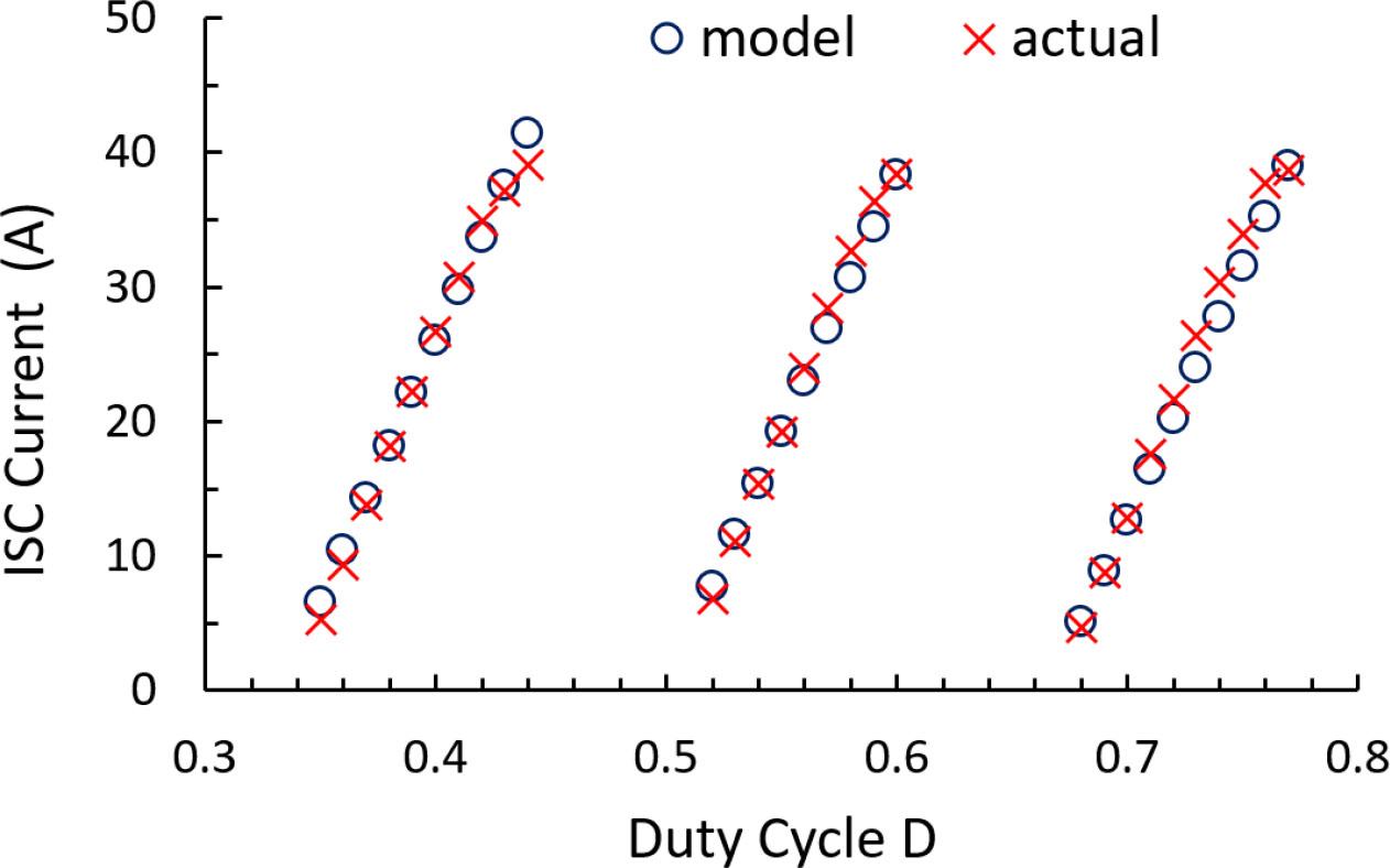
To assess the model performance (Figure 7), Figure 10 presents a comparison between the load current measurements (Figure 5) and those obtained from simulation (Figure 9). A good fit is found, both for variations of D and for the voltage difference (∆V = VIN–VOUT). Furthermore, it is proven that in CCM the static gain measured as the slopes of the graphs is the expected one and that it does not depend on the ∆V.
These results validate the proposed plant model: a first-order system with a gain of 386 and a pole at 107 Hz. Based on this model, it is possible to develop a robust and simple CL control with few resources, as demonstrated in the following subsection.
The objective of the control system is to achieve a good time response and stability using few resources (simplicity criterion). Therefore, we have opted for using an 8-bit µC (PIC18F47Q10). Notice that, due to the options to configure the digital PWM of the selected µC (24 MHz clock frequency and 10-bit resolution) for actual testing in CL, it is used a modulation frequency of 23.437 kHz is used instead of the 20 kHz used for simulations.
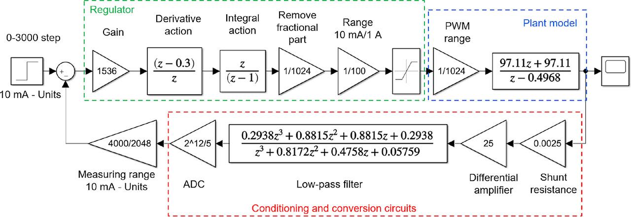
Figure 11 shows the discrete model of the charging current control system, which is programmed using integers (16 bits or 32 bits). The units to work with are the tens of milliamps. Thus, for example, an input step of 30 A is specified with a value of 3,000.
The regulator is programmed in an interrupt routine that is executed every millisecond (sampling frequency of 1 kHz). It consists of a gain that multiplies the error, a derivative action (zero at z = 0.3), an integral with a pole at z = 1 to remove the steady-state position error, and a scaling factor of 1,024. Additionally, it is divided by 100 to go to the ampere range, and it is limited between 0 and 1,023 to avoid overflow in the PWM.
Ideally, considering that the system response can be approximated to that of a second-order system, the position of the zero has been selected so that the root locus crosses through the dominant poles (0.615 ± j0.243) (Figure 12). This results in a time response close to a settling time of 8 ms and an overshoot of 3%. Although, since the other branches of the system also have an influence, the actual response is expected to be slightly worse.
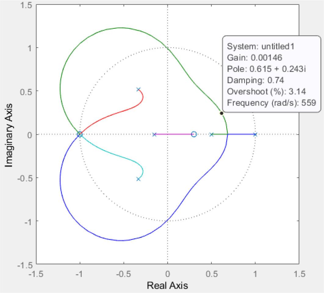
Root locus of the complete system.
According to Eq. (7), applying the Tustin method, the plant model is obtained by discretising the first-order model obtained for the converter (386 for the gain and 107 Hz for the pole).
Moreover, the circuit model includes a new scaling to move to the 0–1 operating range for D. In total, the gain is 1,536 divided by 1,024 twice, that is 0.00146, which is indicated at the root locus in Figure 12.
In the feedback path, there are the Shunt resistance, the differential amplifier and the discrete equivalent of a low-pass filter (cut-off frequency 500 Hz). Finally, it is scaled according to the range (0–5 V) and the ADC bits (MCP3202), and it is converted to units of tens of milliamps.
Figure 13 shows the simulation results. As expected, a settling time close to 8 ms with low overshoot is obtained. It is worth noting that the simulations and practical results are based on CCM operation. Therefore, if it is not operating in this mode, the duty cycle must first be initialised to the value at the limit between DCM and CCM (calculated from the measured input and output voltages). In the unusual case that a very low charging current set point is programmed, and therefore no CCM work is required, the gain of the regulator can be increased so that the response is not too slow.
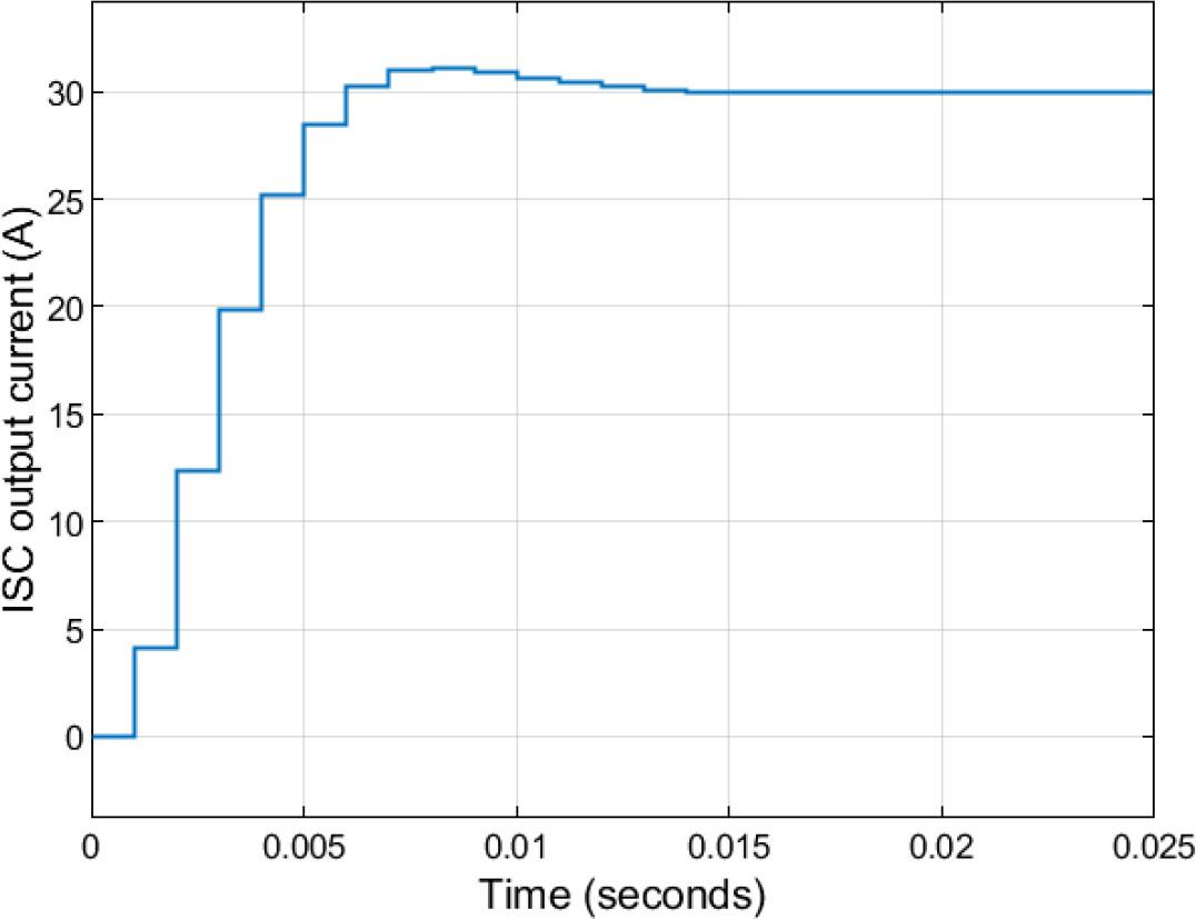
Transient response to an input step of 30 A.
Figure 14 presents the CL experimental results for the initially calculated gain of 1,536 (ISC_1) and for half (ISC_0.5), one quarter (ISC_0.25), and a 10th (ISC_0.1) of that gain. It is observed how it affects the response time and overshoot. It can be concluded that with a gain of one quarter (384) and the classical proportional-integral (PI) compensator, good results have been achieved (response time of 15 ms without overshoot).
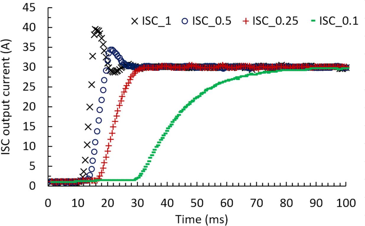
CL transient response to 30 A steps for different gains. CL, closed-loop.
As an example, Figure 15 shows how the output voltage of the SCs responds to a 30 A step charging current. The voltage rises from 20 V to 34 V over a period of 30 s. The typical uncertainty observed is 8.9 mA in the area where the set point has been set to 1 A (within 15 s), and 138 mA in the area where it is at 30 A (between 18 s and 48 s). In low current ranges, this is normal because it is the starting resolution level. And, for high currents it also affects, for example, the noise that is coupled in the measurement circuits and the resolution of the PWM. In any case, these are low relative values (0.9% and 0.5%).
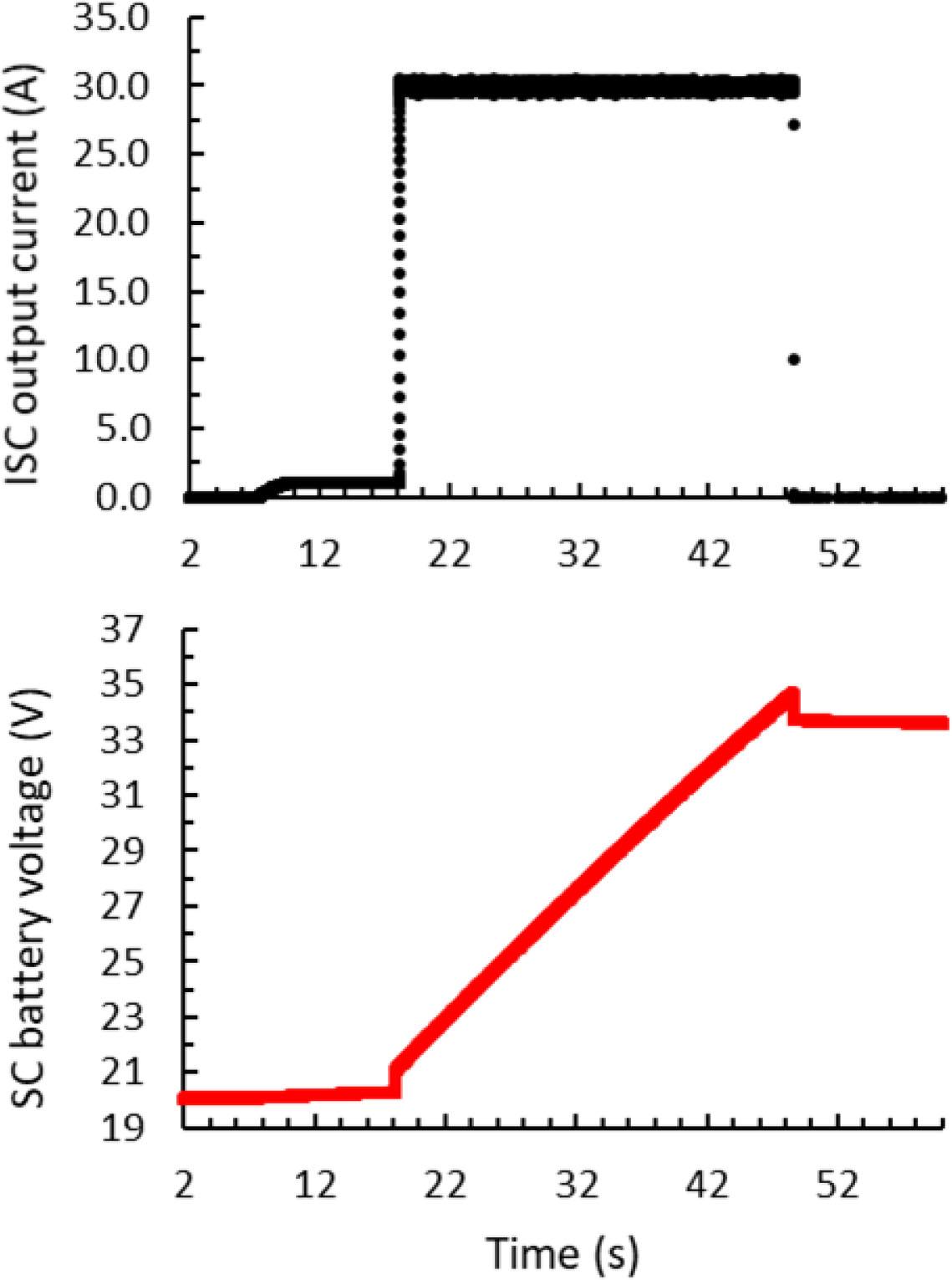
Response to a step from 1 A to 30 A with a gain of 384. SC, supercapacitor.
Table 2 includes a comparison of the step response between this work and several references, demonstrating a rapid response despite the simplicity of the design. This result reveals the importance of relating OL gain to loss resistances.
Step response for different bibliographic references.
| Reference | Step size (A) | Time response (s) | Slope (A/s) |
|---|---|---|---|
| Chen, et al. (2016) | 1 | 0.054 | 18.5 |
| Rigogiannis et al. (2018) | 2.5 | 0.043 | 58 |
| Yang et al. (2019) | 500 | 0.470 | 1,000 |
| Guerriero et al. (2020) | 120 | 0.100 | 1,200 |
| Wang et al. (2021) | 22 | 0.100 | 220 |
| This work | 30 | 0.015 | 2,000 |
The model and its practical implementation of a charging current controller for a SC module based on a buck converter operating in CCM have been presented. With this design, a good settling time (<15 ms) and good stability are achieved with a minimum of hardware and firmware resources. These results have been achieved thanks to a realistic circuit model that has been validated both by simulation and experimentally.
The main novelty of the designed model is that it takes into account all the serial equivalent resistances of the devices and wires to ensure efficient operation in CCM. The effect of these loss resistances of the model on the charging current has been demonstrated, which implies that the model has a high gain, since a small variation in the duty cycle of the PWM controller results in a very large variation of the load current. This realistic model has helped to get a simple and efficient regulator. The practical results of the charger, including its CL operation, demonstrate an adequate behaviour (output steady state variations under 1%), which is achieved with a 10-bit digital PWM and a simple zero-pole pair regulator running on an 8-bit microcontroller with a sampling time of 1 ms. With these minimum resources, the charger exhibits a good performance, which was tested with steps up to 40 A.
The importance of this study is due not only to the good results obtained with the studied model, but also to the possibilities for improvement. On the one hand, it is possible to investigate how to include an estimator of the two circuit parameters to adapt it to possible changes in the loss resistances. For example, due to a change in the wiring or in the SC module that is used. On the other hand, to reduce the output ripple, higher resolution modulators can be evaluated, both of the digital PWM type and others, such as Sigma-Delta modulators. Although in both cases, more resources would be needed.