
Figure 1
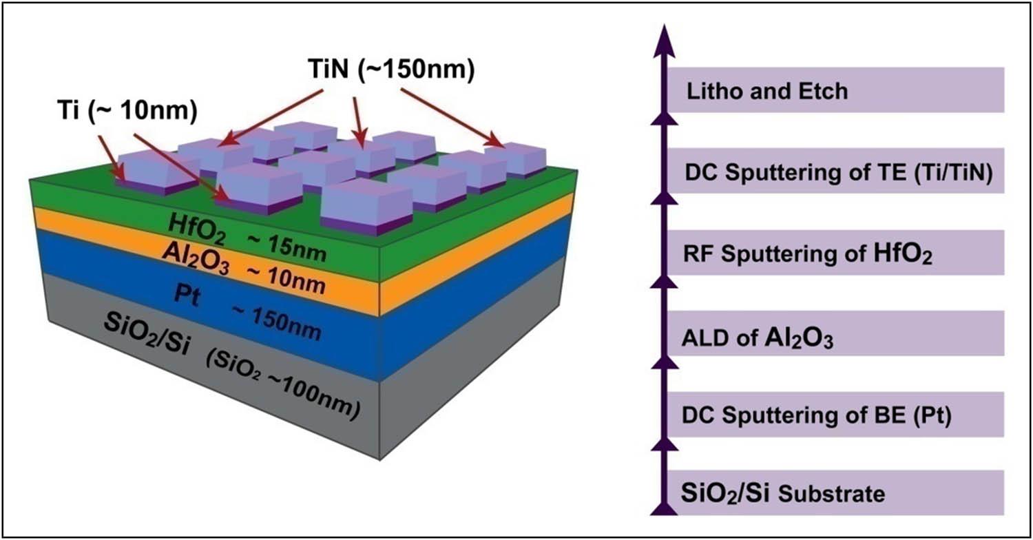
Figure 2
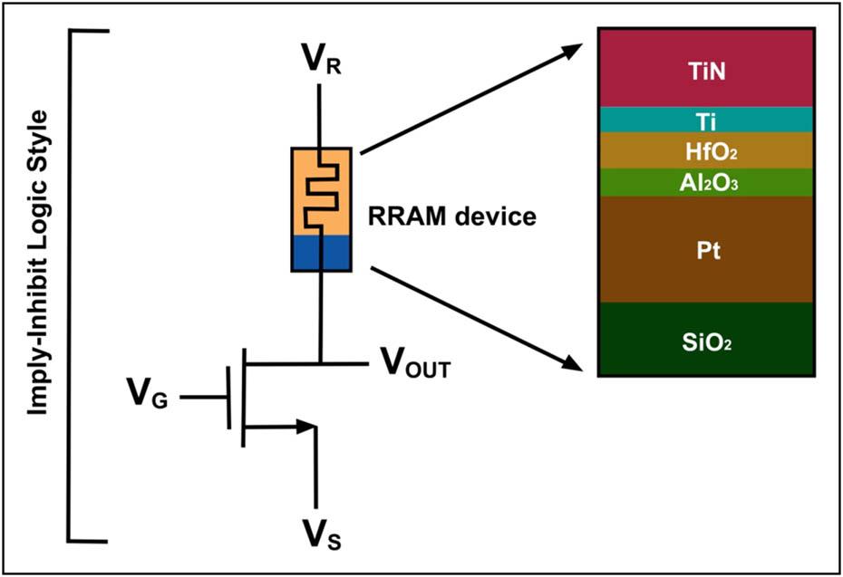
Figure 3
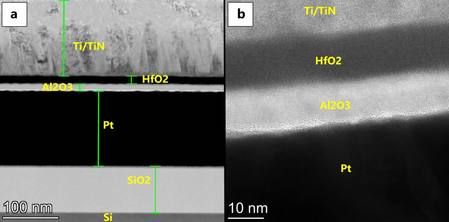
Figure 4
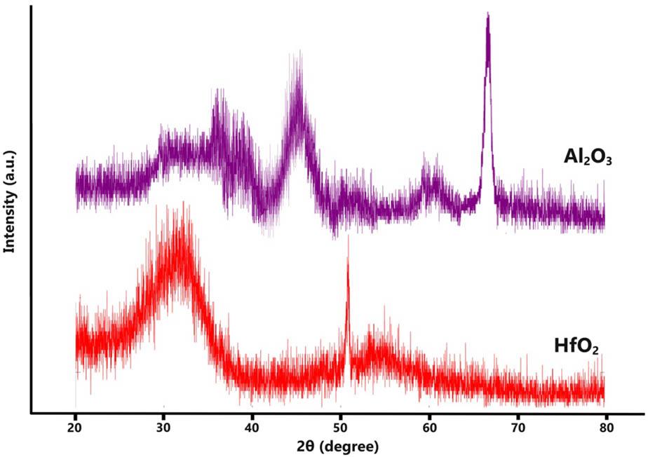
Figure 5

Figure 6
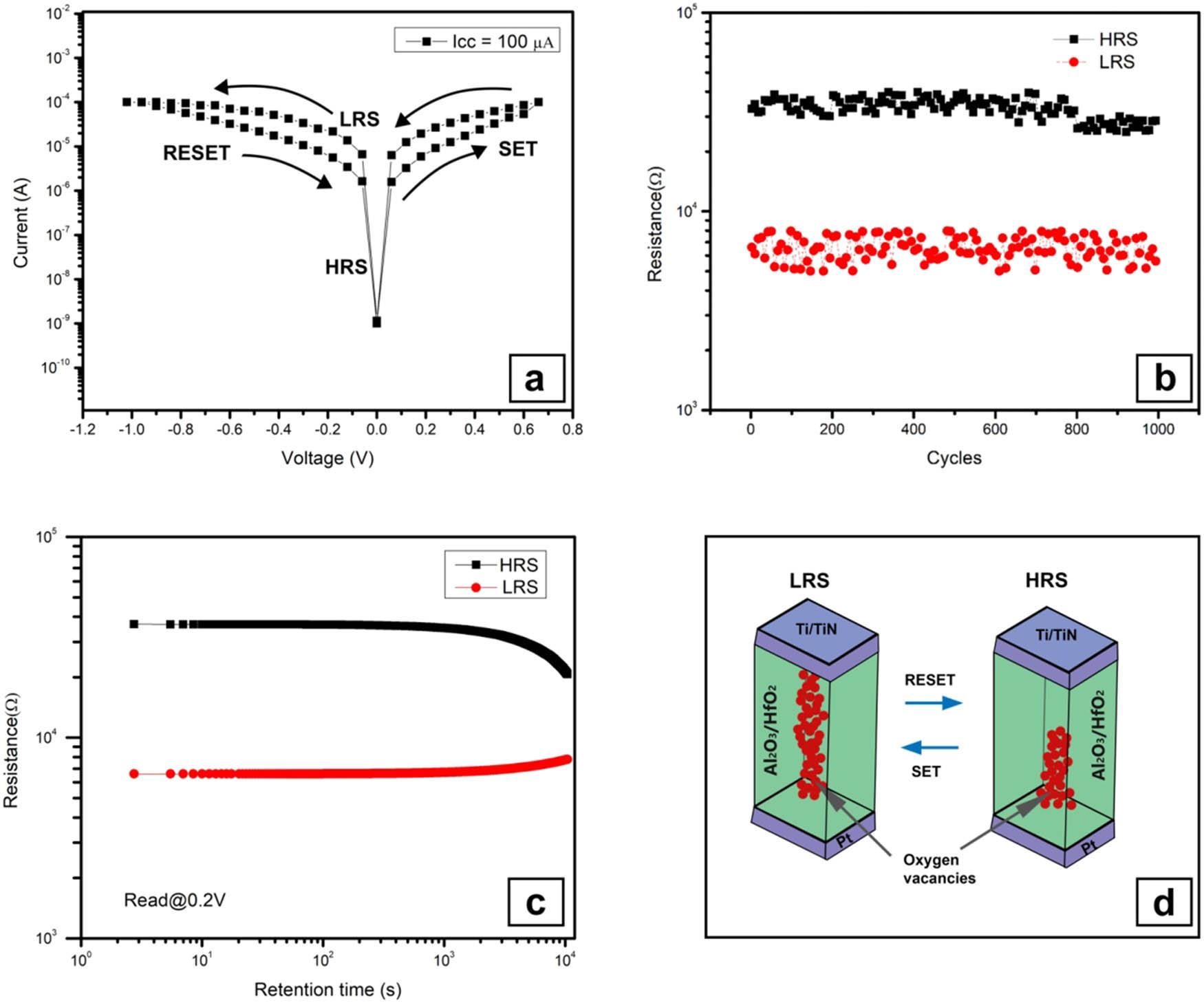
Figure 7
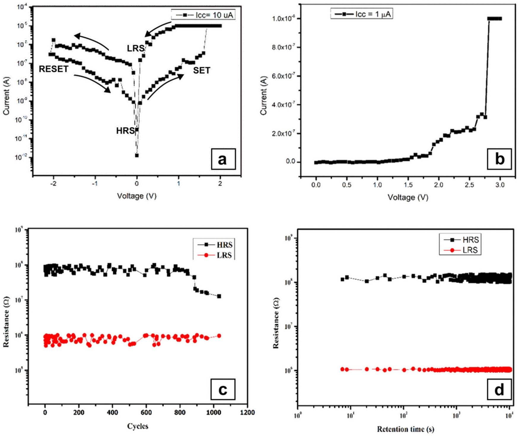
Figure 8

Figure 9

Figure 10
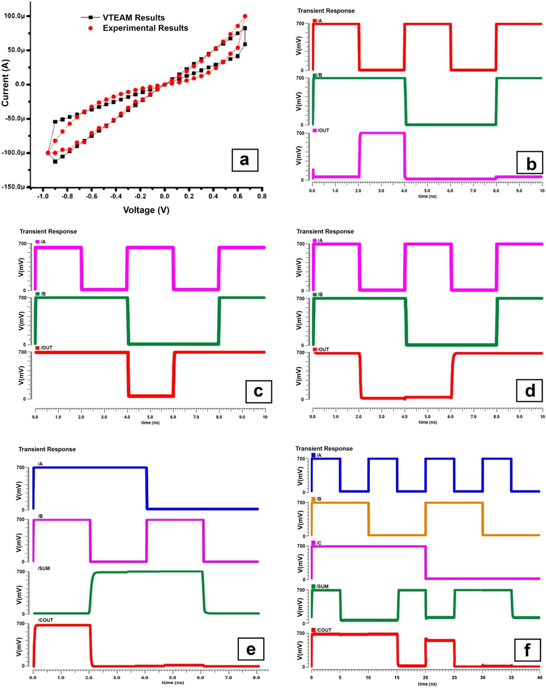
Figure 11
Truth table for simulated logic gates_
| Inputs | Logic gates | |||||||||
|---|---|---|---|---|---|---|---|---|---|---|
| A | B | NOT | AND | OR | IMPLY | INHIBIT | NAND | NOR | XOR | XNOR |
| 0 | 0 | 1 | 0 | 0 | 0 | 1 | 1 | 1 | 0 | 1 |
| 0 | 1 | 1 | 0 | 1 | 1 | 1 | 1 | 0 | 1 | 0 |
| 1 | 0 | 0 | 0 | 1 | 0 | 0 | 1 | 0 | 1 | 0 |
| 1 | 1 | 0 | 1 | 1 | 0 | 1 | 0 | 0 | 0 | 1 |
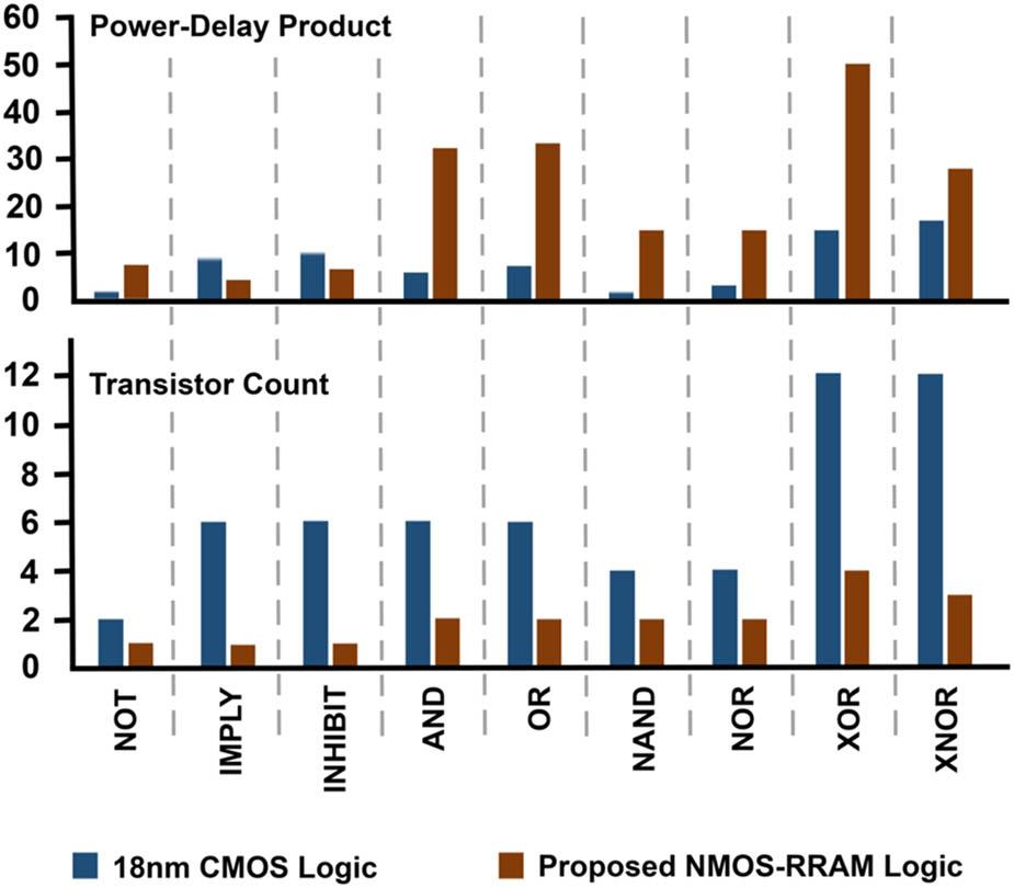
Comparison between proposed memristor-based logic circuits and other logic circuits_
| Function | Logic circuits | Component | Power (µW) | Delay (ps) |
|---|---|---|---|---|
| XOR | 1T2M-based logic [19] | 1T + 6R | 156 | 48.7 |
| Universal logic [20] | 2T + 2R + 1 resistor | 25.77 | 16.74 | |
| MeMOS logic [21] | 4T + 6R | 2.08 | 30.6 | |
| CMOS logic [22] | 8T + 2 inverter | 28.42 | 87.5 × 10³ | |
| Proposed logic | 4T + 4R | 1.955 | 25.6 | |
| XNOR | 1T2M-based logic | 1T + 6R | 168 | 51.7 |
| Universal logic | 2T + 2R + 1 resistor | 36.28 | — | |
| MeMOS logic | 4T + 6R | 2.41 | 31.11 | |
| Proposed logic | 3T + 3R | 1.182 | 23.68 | |
| NOT | 1T2M-based logic | 1T + 2R | 142 | 45.03 |
| MeMOS logic | 2T | 0.5 | 18.7 | |
| CMOS logic | 2T | 0.086 | 13.04 | |
| Proposed logic | 1T + 1R | 0.916 | 7.262 | |
| Half-adder | MeMOS logic | 8T + 8R | 8.07 | 98.05 |
| Proposed logic | 6T + 6R | 1.996 | 42.5 | |
| 1-bit Adder | 1T2M-based logic | 3T + 16R | 307 | 57.93 |
| Universal logic | 16T + 10R + 2 resistor | 134 | 69.3 | |
| MeMOS logic | 16T + 18R | 17.87 | 212.3 | |
| Proposed logic | 7T + 7R | 2.775 | 74.2 | |
| IMPLY | CMOS logic | 6T | 0.218 | 38.91 |
| Proposed logic | 1T + 1R | 0.463 | 7.221 | |
| INHIBIT | CMOS logic | 6T | 0.228 | 42.38 |
| Proposed logic | 1T + 1R | 0.45 | 13.49 |