
The physical limitations of traditional storage devices are driving research toward next-generation non-volatile memory, particularly resistive random access memory (RRAM), owing to its higher density, data persistence, lower power consumption, and simpler structure [1]. The functionality of RRAM relies on resistance changes caused by the formation and deformation of conductive filaments [2]. Therefore, research has focused on the resistive switching phenomenon in various metal-oxide structures [3]. Among the various metal-oxide stacks studied, aluminum oxide (Al2O3)- and hafnium oxide (HfO2)-based bi-layer structures are the most promising for practical applications because the materials used are compatible with complementary metal-oxide-semiconductor (CMOS) processing [4]. The RRAM device consists of metal oxides sandwiched between top electrode (TE) and bottom electrode (BE) materials [5]. Therefore, the optimal selection of TE and BE materials improves the performance, endurance, and retention of RRAM devices. Because of the dominant role of the TE in the reaction with the oxide layer, it has a greater influence on oxygen migration in RRAM than the BE. The barrier height controls the diffusion of oxygen ions into the TE and the formation of an interfacial dielectric layer that governs conducting filament (CF) growth [6]. Studies have demonstrated that the HfO2/TiN contact exhibits a lower barrier height (1.6 eV) than TiN/SiO2 interfaces. This was attributed to the oxygen-binding properties of TiN when used as the TE [7]. In this study, TiN was used as the TE, and a small amount of Ti was doped to improve the functionality of the proposed RRAM devices. The BE is responsible for introducing more vacancies into the oxide layer and providing electrons to improve the conduction mechanism. Pt is the right choice as the BE because it has a high on/off ratio of ∼105 with reduced SET and RESET voltages [8].
This study combined experimental and computational models to investigate a bilayer RRAM device. The device consists of an Al2O3/HfO2 stack sandwiched between Ti/TiN and Pt electrodes. In the experimental section, the fabrication of a bi-layer structure using atomic layer deposition (ALD) and doping of the top and BEs using various sputtering techniques are discussed. Furthermore, modeling of the proposed RRAM device using the VTEAM simulation package is discussed. Section 3 is divided into two parts: one explains the experimental results, and the other discusses the simulation results. In Section 3.1, the nanostructure of the fabricated RRAM device was discussed, which was examined by high-resolution transmission electron microscopy (HRTEM), X-ray diffraction (XRD), and X-ray photoelectron spectroscopy (XPS) studies. In Section 3.2, the electrical performance of the device is then discussed in terms of SET and RESET voltages, compliance currents, high resistance state (HRS), low resistance state (LRS), and endurance in terms of switching cycles. In Section 3.3, the modeling of the RRAM device and the current–voltage (I–V) characteristics obtained from the VTEAM simulation package are discussed. Furthermore, the modeling of imply–inhibit logic gates and their efficiency with respect to existing CMOS devices are analyzed and discussed. Finally, in Section 3, a comparative analysis of the present results with those of existing memristor models is presented.
Figure 1 shows the step-by-step process of fabricating an Al2O3/HfO2 bi-layer RRAM device with a Ti/TiN TE and a Pt BE. The proposed RRAM devices were fabricated in a Class 100 clean room using various deposition techniques. The p-type silicon (Si) substrates were cleaned using a standard Radio Corporation of America process before the deposition of the oxide layers. A 100-nm-thick silicon dioxide (SiO2) layer was grown on the bottom p-type Si substrate with a resistivity of 1–10 Ω using the dry oxidation method. Because dense SiO2 films with thicknesses up to 100 nm can be easily grown in an oxygen-poor environment, the thickness was set to 100 nm [9]. Using the DC sputtering technique, Pt was deposited as the BE at room temperature under a base pressure of 3 × 10⁻⁶ Torr and a working pressure of 6.5 × 10⁻³ Torr. Al2O3 with a thickness of 10 nm was deposited by ALD with trimethylaluminum (TMA), water (H2O), and N2 as purge gases at 250°C. TMA and H2O are the most commonly used precursor systems for ALD of Al2O3 [10]. HfO2 with a thickness of 15 nm was deposited over the Al2O3 layer via RF sputtering in an argon environment.
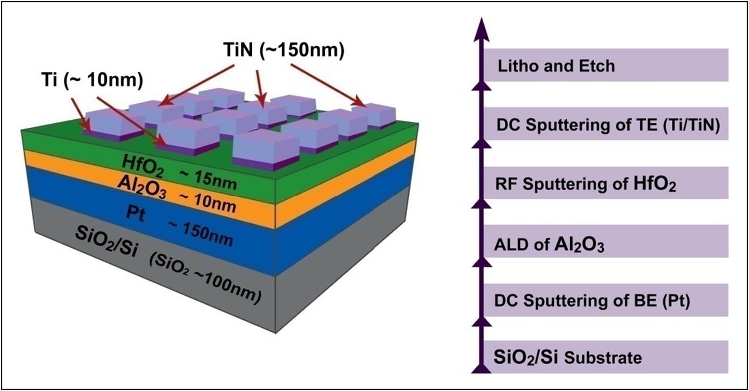
Step-by-step process of fabricating the proposed RRAM device.
Reactive layers of Ti, TiN, or Ta are typically deposited as the TEs to increase the number of defects in the HfO2 layer. This reduces the power of the forming voltage and the SET voltage by reacting with the knocked-out oxygen ions and creating additional oxygen vacancies [11]. In this study, TiN was chosen as the TE, and Ti was added between TiN and HfO2 to increase the number of oxygen vacancies. A Ti cap layer with a thickness of 10 nm and a TiN layer with a thickness of 150 nm were deposited by DC sputtering with a base pressure of 2.3 × 10⁻⁶ and a working pressure of 5.3 × 10⁻³ Torr. After the TE was deposited, lithography and etching were performed using circular patterned masks with a diameter of 100 μm. Finally, post-metallization annealing was performed for 30 min at 400°C in an N2 environment using a rapid thermal annealing technique to improve the contact between the oxide layers and electrodes [5]. The nanostructure cross-section of the Pt/Al2O3/HfO2/Ti/TiN RRAM device was examined using HRTEM, and the binding state and presence of the proposed bi-layer structure were investigated using the XRD peaks and XPS depth profiles. In addition, the electrical performance of the device was examined using SET and RESET voltages, compliance currents, HRS and LRS, and endurance in terms of the switching cycles.
A generic memristor model was used to investigate the compatibility of the proposed RRAM device for imply–inhibit logic operations. Several memristor models have been proposed [12]. Among them, the VTEAM model is perfect for logic design. It is more general and simpler and has a physical concept similar to the Simmons tunnel barrier model [13]. The only difference is that a voltage threshold is used instead of a threshold current, and the derivative of the internal state variable is used.
The proposed RRAM device is ideal for the VTEAM simulation model because of its free-forming characteristics. The modeling parameters considered were threshold voltages, conductive filament gaps, temperature, and device growth dynamics. A voltage-controlled time-invariant memristive device is generally represented by the linear dependence of the resistance and the state variable derivative [13]
The Cadence Virtuoso was used to implement and simulate the proposed design. The transistors used in the design were based on 18 nm N-channel metal-oxide-semiconductor (NMOS) devices. Verilog-A coding was used to derive the I–V characteristics of the proposed device. In the proposed model shown in Figure 2, an RRAM device is positioned at the drain of the NMOS device and acts as a pull-up device, whereas the NMOS acts as a pull-down device. The NMOS is in the off state, and VOUT is charged to VDD via RRAM when the gate voltages are complementary gate voltage (VG) = 0, source voltage (VS) = GND, and RRAM voltage (VR) = VDD. Similarly, the NMOS is in the ON state, and VOUT discharges to the ground through the NMOS device when VG = 1, VS = GND, and VR = VDD. Therefore, the proposed 1T–1R structure acts as an inverter using an NMOS transistor (1T) with VG = input and VS = 0 and RRAM (1R) as a potential divider with VR = VDD. By adjusting the VR and VS voltages, the proposed structure can be used to implement imply–inhibit logic gates.
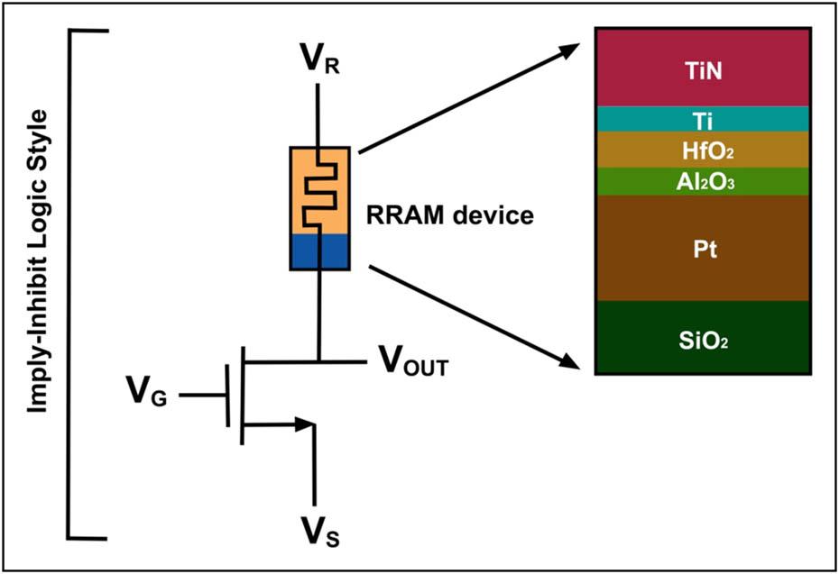
Proposed 1T-1R structure for imply–inhibit logic gates.
The nanostructure and interfacial morphologies of the proposed Al2O3/HfO2 bi-layer RRAM device were investigated using HRTEM. Figure 3(a) shows the cross-section of the Pt/Al2O3/HfO2/Ti/TiN bilayer RRAM structure. At the bottom of the image, SiO2 was deposited on an Si base with a thickness of ∼103.4 nm. Pt of the BE is deposited over an SiO2 layer with a thickness of ∼142 nm and is easily recognized by its gray color. The bi-layer structures of Al2O3 and HfO2 have thicknesses of ∼12.77 and ∼15.17 nm, respectively. In the TE, the interface region between the TiN and Ti layers appeared in a similar color (total width of ∼162 nm), which is why the interface between the two layers was not correctly identified. Overall, it was confirmed that the total thickness of the proposed device was approximately 332 nm, which was comparable to the target thickness of 335 nm. The laminated structures of Pt/Al2O3/HfO2/Ti/TiN from bottom to top are shown in Figure 3(b). The image also shows that there are no overlaps or major defects at the interface between the oxide layers.
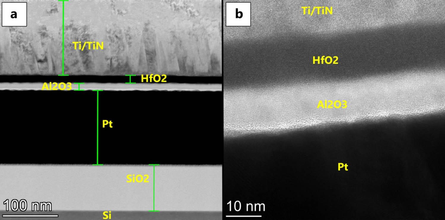
(a) Cross-sectional HRTEM image of the Pt/Al2O3/HfO2/Ti/TiNbi-layer RRAM structure. (b) The closer view of layer deposition and its interface.
XRD analysis was performed to investigate the presence of the Al2O3/HfO2 bilayer structure. Figure 4 shows the XRD patterns of the Al2O3 and HfO2 metal oxide films. In the Al2O3 diagram, the first 2θ peak is indexed at 33°, followed by four peaks at 37°, 39°, 46°, and 68°. The peaks and corresponding angles agreed well with the standard JCPDS-ICDD-card number 00-046-1131 [14]. The 2θ peaks identified at 32° and 51° in Figure 4 confirm the presence of HfO2 and matched JCPDS-ICDD card number 00-006-0318. The broad peak of HfO2 at 32° on the 2θ scale indicated that the layer had more oxygen vacancies [15].
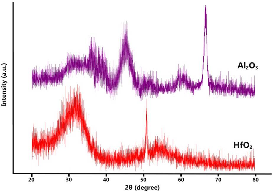
XRD pattern of Al2O3 and HfO2 nanoparticles.
To obtain a deeper understanding of the switching mechanism of the proposed bi-layer, we performed an XPS analysis of the Al2O3/HfO2 structures. Narrow-scan XPS spectra of the Al 2p, Hf 4f, and O 1-s peaks of the Al2O3 and HfO2 films are shown in Figure 5. The Al2p peak is at 72.9 eV, which is due to the Al–O bond (Figure 5(a)). The Hf4f peak, attributed to the Hf–O bond, is spotted with doublet peaks of Hf 4f5/2 and Hf 4f7/2 at 16.3 and 14.9 eV (Figure 5(b)). The spin–orbit distance between the 4f5/2 and 4f7/2 peaks is 1.6 eV and is compatible with the literature data of high-k HfO2 [16]. The slightly lower binding energies of the O 1-s peak at 529.9 and 529.1 eV, which correspond to the Al–O and Hf–O bonding in the Al2O3 and HfO2 layers, respectively (Figure 5(c) and (d)). The XPS peak of the 1s peak in HfO2 appeared as unsymmetrical and therefore deconvoluted the peaks. The results clearly demarcate the existence of oxygen vacancies.
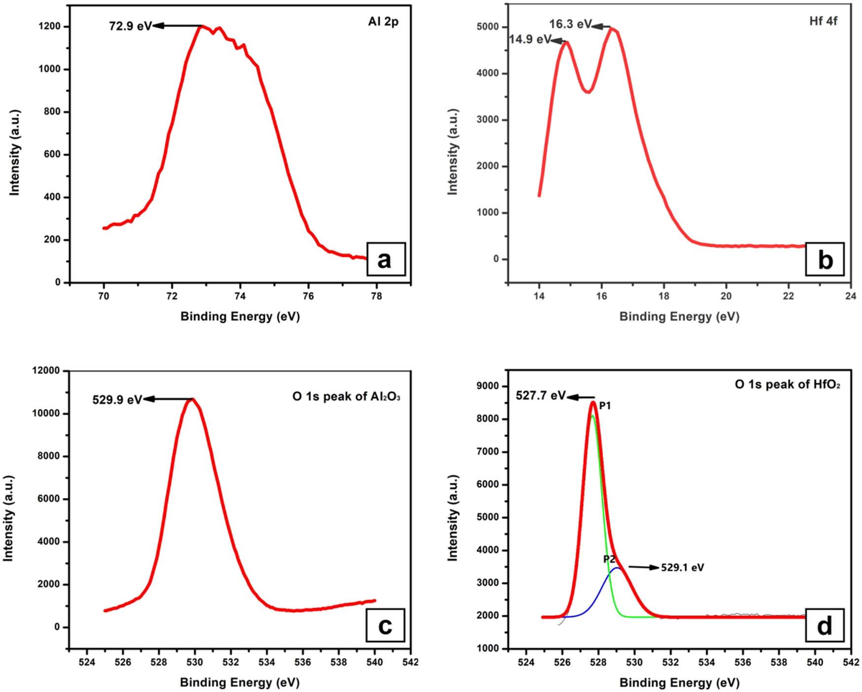
XPS spectra of the Al2O3/HfO2 bi-layer structure. (a) Al2p, (b) Hf4f peaks, (c) O 1-s peak of the Al2O3 layer, and (d) O 1-s peak of the HfO2 layer.
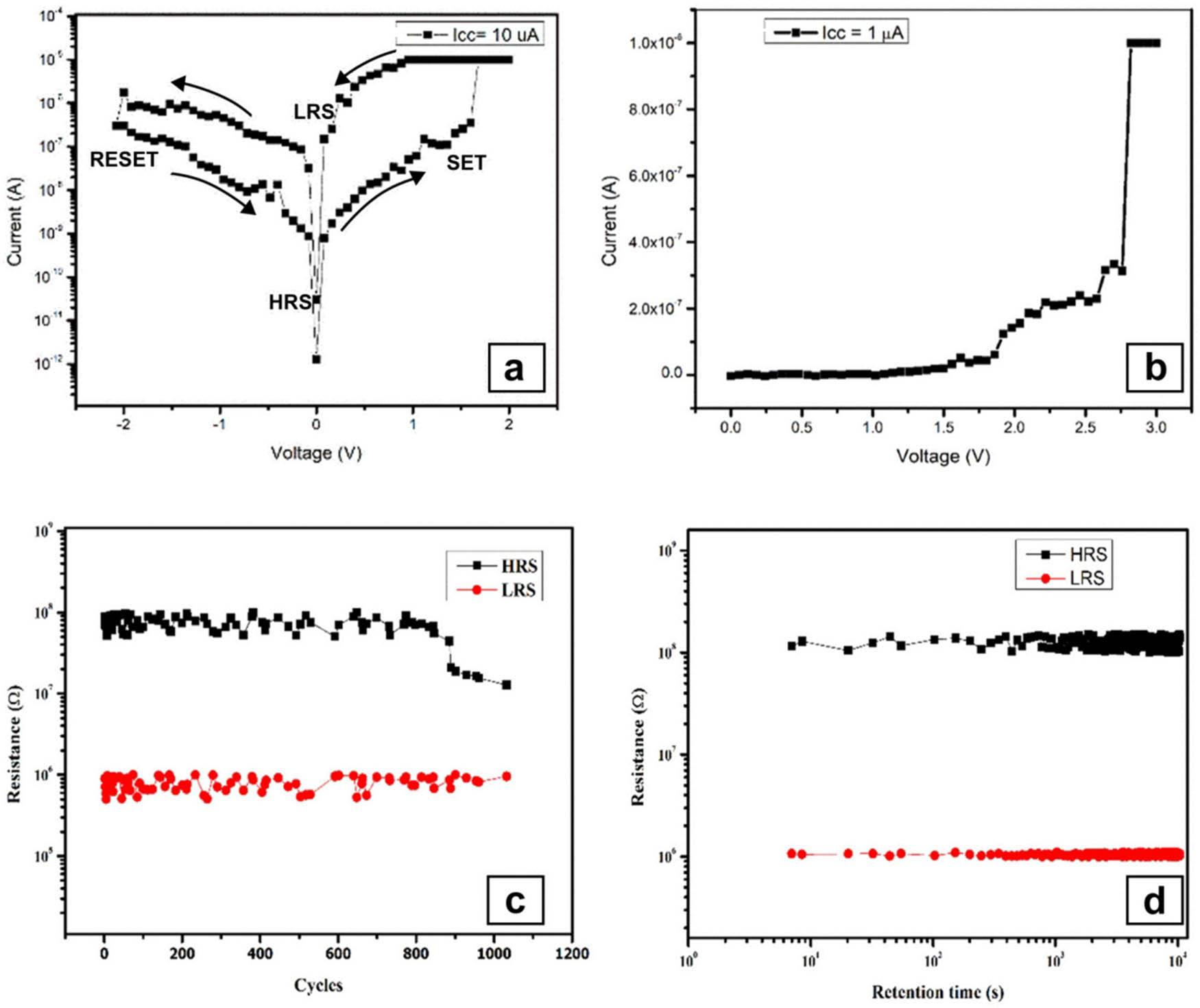
Typical I–V characteristics of the proposed RRAM device with Ti/TiN as the TE and Pt as the BE are shown in Figure 6(a). The curve shows reduced SET (0.66 V) and RESET (−0.9 V) voltages with 100 µA as compliance current. The voltage required to achieve filament formation (forming voltage) decreases with increasing Ti content [17]. The creation and deformation of CF primarily regulate the resistance switching in the interfacial layers. The HfO2 oxide layer is oxygen vacancy rich; therefore, the CF size in the HfO2 layer is larger than that in the Al2O3 layer. Therefore, the addition of a Ti capping layer (CL) between the TiN and HfO2 layers creates more oxygen vacancies. An increase in the oxygen vacancy defect concentration in the active layer promotes the formation of CF without an electroforming voltage, resulting in the forming free device [18]. Therefore, the inclusion of a Ti layer tends to minimize the SET and RESET voltages of the proposed RRAM device with forming-free characteristics. In addition, the device exhibits an endurance of 103 switching cycles with a read voltage of 0.2 V and a resistance on/off ratio of ∼10, as depicted in Figure 6(b) and (c). The resistive switching mechanism of the proposed RRAM device is mainly dominated by the formation and rupture of CFs of oxygen vacancies in the interfacial layers (Figure 6(d)).

Resistive switching characteristics of the device unit and distribution of the SET and RESET voltages. (a) Typical resistive switching characteristics of the device, (b) durability of the device unit, (c) memory retention of HRS and LRS for 103 s with a read voltage of 0.2 V, and (d) resistive switching mechanism of the Pt/Al2O3/HfO2/Ti/TiN RRAM during the SET and RESET process.
The linkage or rupture of the conductive filaments corresponds to SET from the HRS to the LRS or RESET from the LRS to the HRS, respectively. The CF is a channel with a very small diameter of the order of nanometers that connects the top and BEs of the memory cell. An LRS with high conductivity was obtained when the filament was connected, and an HRS occurred when the filament was disconnected from the gap between the electrodes.
In order to show the effectiveness of the present device, the electrical performance of the Pt/Al2O3/HfO2/TiN memristor was examined, and the results were compared. The I–V characteristics of the TiN-top device without a CL, measured with a compliance current of 10 µA, show asymmetrical SET and RESET characteristics as illustrated in Figure 7a and exhibit an SET voltage of 1.13 V and a RESET voltage of −1.8 V, with a compliance current of 100 µA. The use of Al₂O₃, which has a lower activation energy (1.8 eV) compared to HfO₂ (4.6 eV), as a buffer layer significantly reduces the dielectric power of the device. The typical I–V graph shown in Figure 7a indicates that the device with a Ti CL achieves lower SET (0.66 V) and RESET (−0.9 V) voltages compared to the device without a CL, with a compliance current of 100 µA. The TiN-top device without a CL requires a forming voltage of >2 V (Figure 7b), which demonstrates lesser forming-free behavior.
Resistive switching characteristics of the Pt/Al2O3/HfO2/TiN device. (a) Typical I–V characteristics of the device, (b) forming behavior, (c) durability of the device, and (d) memory retention of HRS and LRS for 103 s with a read voltage of 0.2 V.
Ti is employed as a buffer layer between TiN and HfO₂ because it is more reactive to oxygen than TiN. Oxygen ions react with the Ti layer to form a reactive Ti-oxide compound, leaving behind oxygen vacancies that facilitate the formation of CFs without the need for an electroforming voltage, resulting in a forming-free device. Consequently, the inclusion of the Ti CL effectively reduces both the SET and RESET voltages. For TiN-top devices, endurance was measured for 1,000 repetitive cycles under DC sweeps of 0–2 V for SET and 0 to −2 V for RESET, with resistance values read at 0.2 V. The TiN-top device without a CL maintained a memory window of 1,000 for 600 cycles, which gradually reduced to <100 by the 1,000th cycle (Figure 7c), while the TiN-top with a CL demonstrated a stable resistive window of ∼10, enhanced uniformity due to forming-free characteristics, and an annealing procedure. Both devices exhibited a retention time of 104 s, with consistent HRS and LRS values throughout this period (Figure 7d).
The cycle-to-cycle variation in I–V characteristics of Pt/Al2O3/HfO2/TiN shows the switching voltage varied between 1.5 and −2 V (Figure 8a). Alongside, the Pt/Al2O3/HfO2/Ti/TiN device exhibits reduced SET (0.66 V) and RESET (−0.9 V) voltages compared to the TiN-top device without CL (Figure 8b). The device-to-device consistency was examined for the TiN-top device with and without a Ti CL. The TiN-top device without CL exhibits SET voltages distributed between 0.9 and 1.28 V, while RESET voltages range from −1.2 to −2.75 V, showing significantly higher variation in RESET voltages (Figure 8c and d). In contrast, the TiN-top device with CL shows SET voltages distributed from 0.6 to 0.82 V (mean centered at 0.66 V) and RESET voltages from −0.84 to −0.98 V (mean centered at −0.9 V), indicating much narrower distributions (Figure 8e and f). These findings highlight that precise control over material properties, forming-free mechanisms, and annealing processes is crucial for achieving improved device-to-device uniformity.

(a) Cycle-to-cycle variation in I–V characteristics of Pt/Al2O3/HfO2/TiN device, (b) cycle-to-cycle variation in I–V characteristics of the Pt/Al2O3/HfO2/Ti/TiN device, (c) and (d) SET and RESET voltage distribution of the Pt/Al2O3/HfO2/TiN device, and (e) and (f) SET and RESET voltage distribution of the Pt/Al2O3/HfO2/Ti/TiN device.
VTEAM was used to develop a model for Pt/Al2O3/HfO2/Ti/TiN based on the linear dependence of the resistance and state variable equations [13]. The proposed 1T-1R structure (Figure 2) acted as an imply and inhibit logic gate with respect to voltage parameters such as the VR, VG, and VS. The product of the VR and the VG provides the output for the imply style logic gate. By assigning the pulsed inputs VG as A and VR as B and the VS as GND, the output result (Vout) is A′B. Similarly, the sum of the VG and VS voltages provides the output of the inhibit style logic. By assigning two pulsed inputs VG as A, VS as B, and VR = VDD, Vout was A′ + B. In this case, the output becomes zero only when A = 1 and B = 0 because all other nodes are connected to high logic levels without being grounded.
The basic AND and OR gates are implemented using imply and inhibit logic gates. The AND gate is created by supplying two inputs A′ and B to the imply gate, and similarly, the OR gate is created by supplying two inputs A′ and B to the inhibit gate. The NAND and NOR gates are implemented by complementing the RRAM input VR for the NAND gate and source input VS for the NOR gate, respectively. The XNOR gate is implemented by connecting the inhibit logic gate A′ + B to the RRAM node VR and the imply logic gate A′B to the gate input VG, providing the source voltage of the transistor to be grounded. The XOR gate is derived by complementing the XNOR gate. The truth tables for the above-discussed logic gates are shown in Table 1. The 1T–1R structure can be utilized to build complex logic circuits. The half-adders are designed using XOR gates and AND gates similarly. Figure 9 shows the circuit diagram for a 1-bit adder is a combination of Imply, Inhibit, and XNOR gates.
Truth table for simulated logic gates.
| Inputs | Logic gates | |||||||||
|---|---|---|---|---|---|---|---|---|---|---|
| A | B | NOT | AND | OR | IMPLY | INHIBIT | NAND | NOR | XOR | XNOR |
| 0 | 0 | 1 | 0 | 0 | 0 | 1 | 1 | 1 | 0 | 1 |
| 0 | 1 | 1 | 0 | 1 | 1 | 1 | 1 | 0 | 1 | 0 |
| 1 | 0 | 0 | 0 | 1 | 0 | 0 | 1 | 0 | 1 | 0 |
| 1 | 1 | 0 | 1 | 1 | 0 | 1 | 0 | 0 | 0 | 1 |
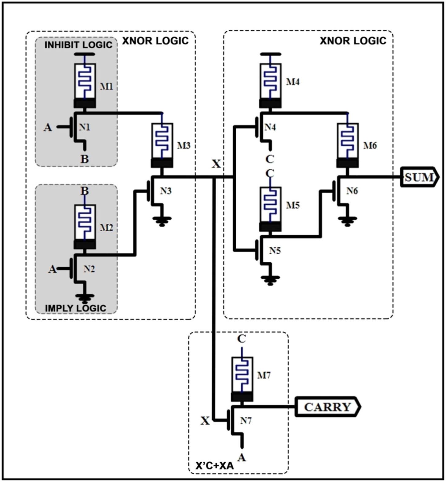
The circuit diagram for a 1-bit adder with a combination of inhibit, imply, and XNOR logic gates.
The I–V characteristics of the proposed RRAM device were derived using an annealing algorithm, and an RMS error of 0.02% was achieved. Figure 10(a) shows the hysteresis curve of the simulation results superimposed on the experimental results. The SET and RESET voltages of the simulated results matched the experimental results and loop structure in a similar manner. Imply and inhibit logic gates were implemented with 18 nm technology using the Cadence Virtuoso software. The circuit was simulated for the inverter design with rise time tr = 10 ps, fall time tf = 10 ps, delay td = 50 ps, period tp = 4 ns, and pulse width tpw = 2 ns. A transient simulation was performed for 10 ns. The average delay for the inverter is calculated by taking the average of the high-to-low and low-to-high propagation delays. The simulated waveforms of the imply, inhibit, and XNOR, half-adder, and full-adder logic gates are shown in Figure 10(b)–(d).
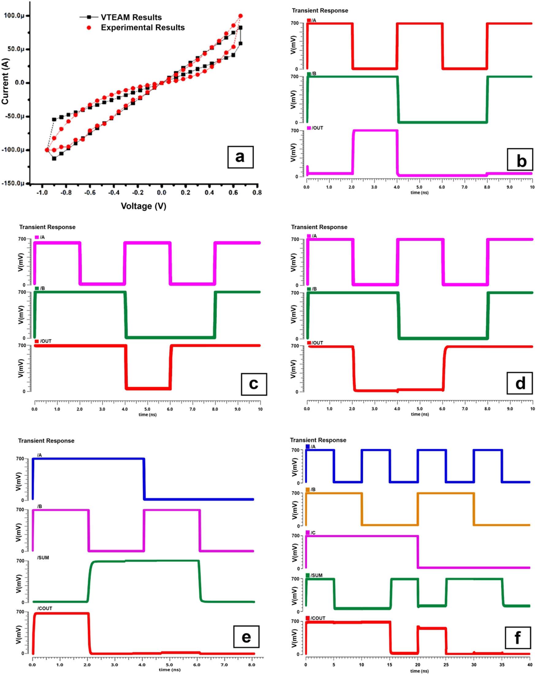
(a) Hysteresis curve of the simulation results superimposed on the experimental results, (b) simulated waveform of imply logic, (c) simulated waveform of inhibit logic, (d) simulated waveform of XNOR logic, (e) simulated waveform of half-adder, and (f) simulated waveform of full-adder.
Table 2 compares the components, time delay, and power consumption of the proposed logic circuit with those of available logic circuits. In the proposed logic, 1T−1R devices were used to implement the logic functions. The components used to design the circuit in other logic styles were high compared with the proposed logic style. The increasing use of transistors for circuit design has led to a slowdown in the operating speed. Although the proposed logic expresses power consumption, it results in low power and delay for the half-adder, imply, and inhibit logic gates. The proposed logic exhibits a leakage current that could be mitigated by increasing the width of the NMOS transistor. Complex logic circuits with smaller areas and delays can be implemented by further extending this logic. The power delay product (PDP) comparison in Figure 11 shows that imply–inhibit logic is area efficient compared to the traditional CMOS logic style in terms of size and delay. In addition, the transistor count shows that the proposed logic utilizes a minimal number of transistors compared with CMOS logic.
Comparison between proposed memristor-based logic circuits and other logic circuits.
| Function | Logic circuits | Component | Power (µW) | Delay (ps) |
|---|---|---|---|---|
| XOR | 1T2M-based logic [19] | 1T + 6R | 156 | 48.7 |
| Universal logic [20] | 2T + 2R + 1 resistor | 25.77 | 16.74 | |
| MeMOS logic [21] | 4T + 6R | 2.08 | 30.6 | |
| CMOS logic [22] | 8T + 2 inverter | 28.42 | 87.5 × 10³ | |
| Proposed logic | 4T + 4R | 1.955 | 25.6 | |
| XNOR | 1T2M-based logic | 1T + 6R | 168 | 51.7 |
| Universal logic | 2T + 2R + 1 resistor | 36.28 | — | |
| MeMOS logic | 4T + 6R | 2.41 | 31.11 | |
| Proposed logic | 3T + 3R | 1.182 | 23.68 | |
| NOT | 1T2M-based logic | 1T + 2R | 142 | 45.03 |
| MeMOS logic | 2T | 0.5 | 18.7 | |
| CMOS logic | 2T | 0.086 | 13.04 | |
| Proposed logic | 1T + 1R | 0.916 | 7.262 | |
| Half-adder | MeMOS logic | 8T + 8R | 8.07 | 98.05 |
| Proposed logic | 6T + 6R | 1.996 | 42.5 | |
| 1-bit Adder | 1T2M-based logic | 3T + 16R | 307 | 57.93 |
| Universal logic | 16T + 10R + 2 resistor | 134 | 69.3 | |
| MeMOS logic | 16T + 18R | 17.87 | 212.3 | |
| Proposed logic | 7T + 7R | 2.775 | 74.2 | |
| IMPLY | CMOS logic | 6T | 0.218 | 38.91 |
| Proposed logic | 1T + 1R | 0.463 | 7.221 | |
| INHIBIT | CMOS logic | 6T | 0.228 | 42.38 |
| Proposed logic | 1T + 1R | 0.45 | 13.49 |

PDP and transistor count comparison between proposed logic style and CMOS logic style.
A comparative analysis of the proposed imply–inhibit logic with other known memristor-based logics was performed. Compared with the proposed logic device, CMOS logic is inefficient in terms of area because it uses many transistors [22]. The proposed logic device requires fewer computational steps to implement gates than the imply logic style [23]. The hybrid logic used PMOS and NMOS devices, whereas the proposed logic uses NMOS transistors and RRAM devices to make the logic area more efficient [24]. The basic gates are easily implemented in the MRL logic style; however, other gates require a CMOS inverter [25]. Likewise, writing, reading, and resetting in MAGIC logic style require additional circuit design. There are also design limitations for crossbar implementation [26]. The threshold-logic style causes signal degradation and requires a CMOS inverter [27]. The device requires an additional drive circuit in MAD logic style. However, the proposed logic style works effectively without this. CMOS-like memristor logic requires CMOS and voltage drivers as additional components and has complex circuitry [28]. Compared to all other logic styles, as shown in Table 2, the proposed imply–inhibit logic-based circuits provide efficient results with reduced time delays. The experimental and simulation results of the proposed RRAM device showed reduced SET and RESET voltage and resistance values, which are ideal for the implementation of the imply–inhibit logic style. The proposed imply–inhibit logic gate provides effective results with less time delay than other logic designs. The experimental and simulation results of the proposed RRAM device show lower SET and RESET voltage and resistance values, which are ideal for implementing the imply–inhibit logic style.
A Pt/Al2O3/HfO2/Ti/TiN bilayer RRAM device was fabricated, and its compatibility with imply inhibit logic applications was studied. The presence of layers in the Al2O3/HfO2 bilayer structure was confirmed by the cross-sectional HRTEM images and XPS depth profiles. The resistance switching behavior of the Pt/Al2O3/HfO2/Ti/TiN memory device was studied, and the results showed a stable resistance ratio (∼10) of the ON/OFF states, sharp distribution of the SET and RESET voltages, better switching endurance up to 103 cycles, and longer data retention. The Ti interface between HfO2 and TiN plays an important role in improving the resistance switching properties. The VTEAM model was used to fit the I–V curve between the experiment and simulation and achieved a perfect fit with 0.02 RMS errors. The proposed imply and inhibit logic gates were computed and simulated using Cadence Virtuoso 18 nm technology. The results were compared with those of existing memristor logic and showed better performance, delay, and device count characteristics.
Part of the research was conducted at CeNSE Lab, IISc Bangalore-India under the INUP program funded by the Ministry of Electronics and Information Technology (MeitY), Government of India, and NN acknowledged SEED fellowship funded by Kumaraguru College of Technology, Coimbatore.
Authors state no funding involved.
Nithya Natarajan: Conceptualization, Original draft preparation, Methodology, Data curation, Experiment and Simulation investigations. Paramasivam Kuppusamy: Supervision, Reviewing and Editing, Validation.
The authors declare that they have no known competing financial interests or personal relationships that could have appeared to influence the work reported in this paper.