
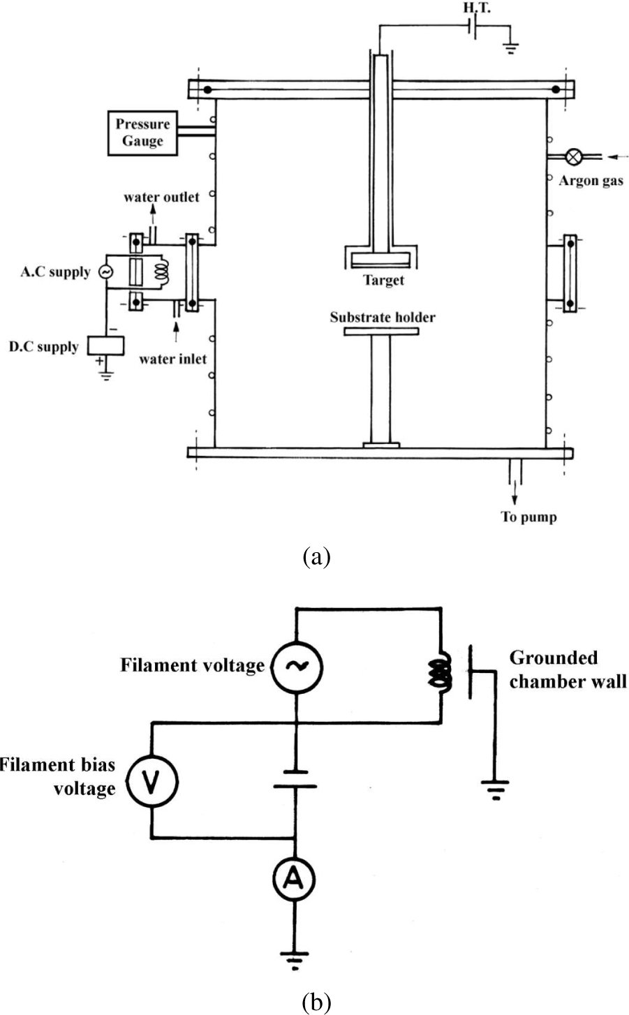
(a) schematic diagram of DC magnetron sputtering with supported discharge, (b) electrical circuit diagram of the supported discharge.
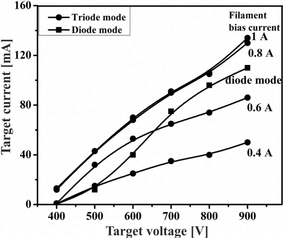
Voltage-current characteristics in diode mode and triode mode at different filament bias currents.
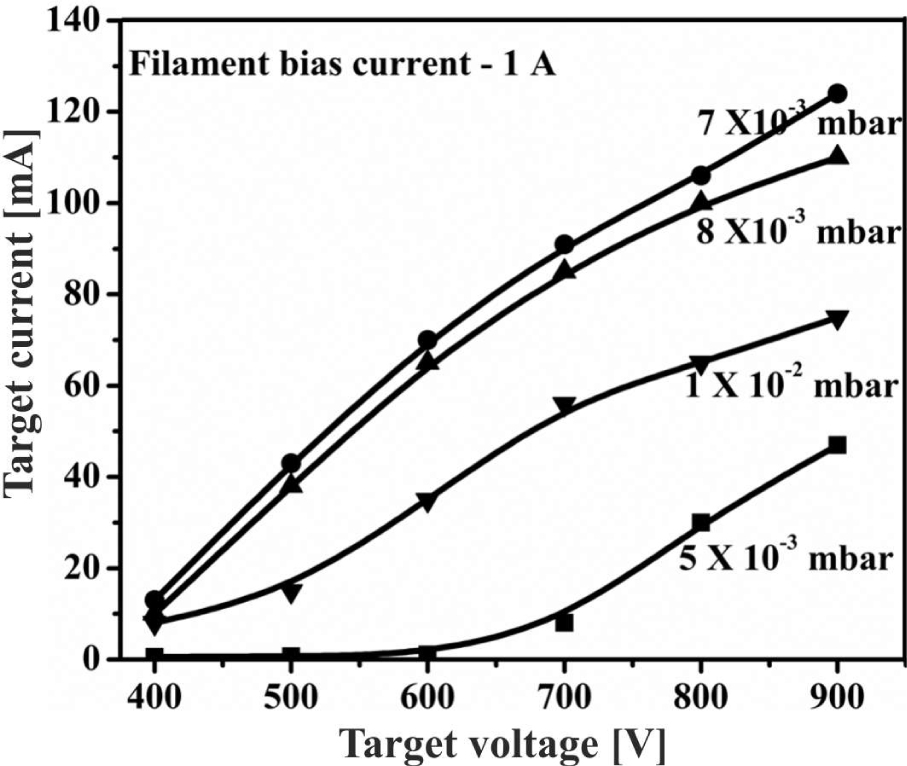
Variation of target current with target voltage at a constant filament bias current of 1.0 A for different pressures.
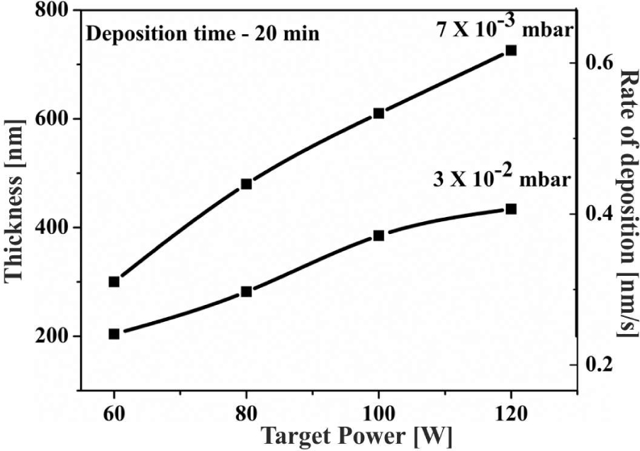
Variation of thickness/rate of deposition on target power for the films deposited in diode and supported discharge modes, for dS−T = 4 cm.
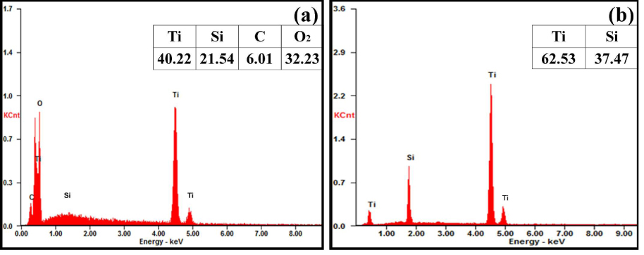
EDS spectra for the Ti thin films deposited at (a) 3 Pa and (b) 0.7 Pa.
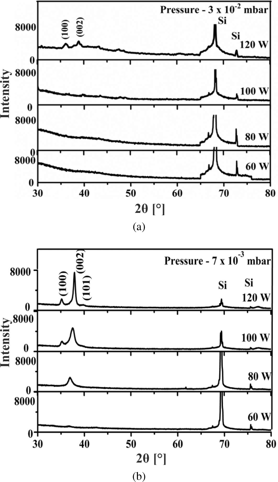
XRD patterns of Ti thin films deposited at a pressure of (a) 3 Pa, (b) 0.7 Pa at different target powers.
Table 1
Qualitative analysis of crystallite size.
| Working pressure [Pa] | Target power [W] | Grain size [nm] | Relative intensity [%] | Surface roughness [nm] |
|---|---|---|---|---|
| 80 | 64 | 36 | 7 | |
| 0.7 | 100 | 65 | 62 | 12 |
| 120 | 80 | 100 | 15 | |
| 80 | 12 | 8 | 2 | |
| 3 | 100 | 13 | 9 | 4 |
| 120 | 20 | 12 | 5 | |
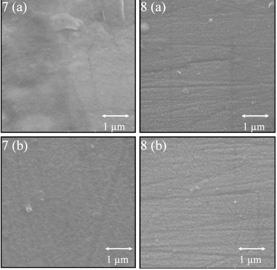
SEM images of Ti thin films deposited in diode mode at the target power of (a) 60 W, (b) 80 W, (c) 100 W and (d) 120 W.
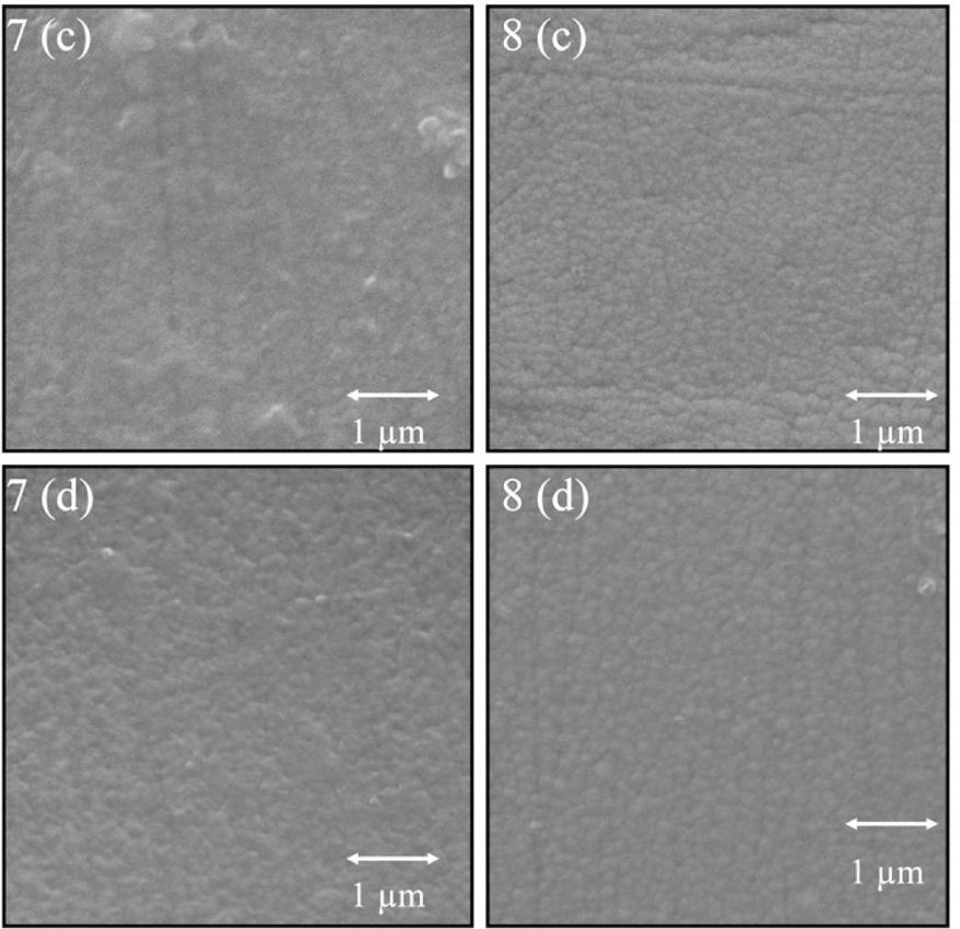
Ti thin films deposited in triode mode at the target power of (a) 60 W, (b) 80 W, (c) 100 W and (d) 120 W.
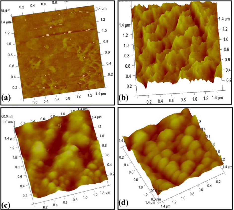
AFM images of Ti films deposited in supported discharge system at the target power of (a) 60W, (b) 80 W, (c) 100 W and (d) 120 W.
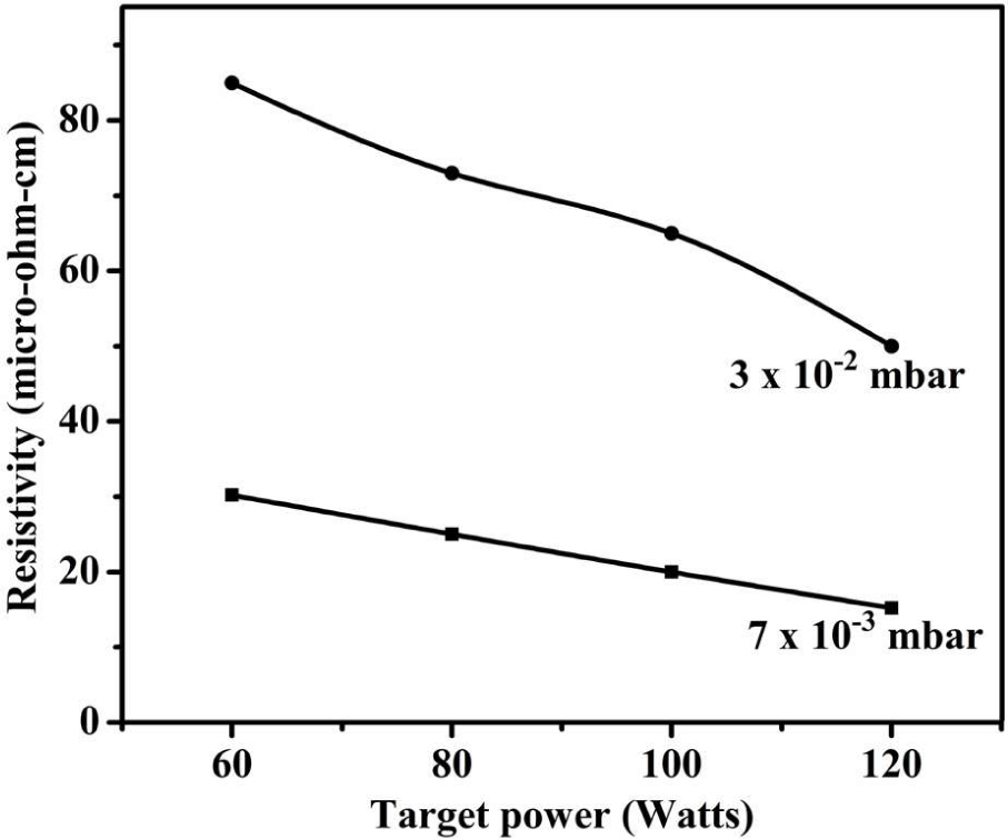
Variation of electrical resistivity with target power of Ti thin films deposited in diode and triode mode.