
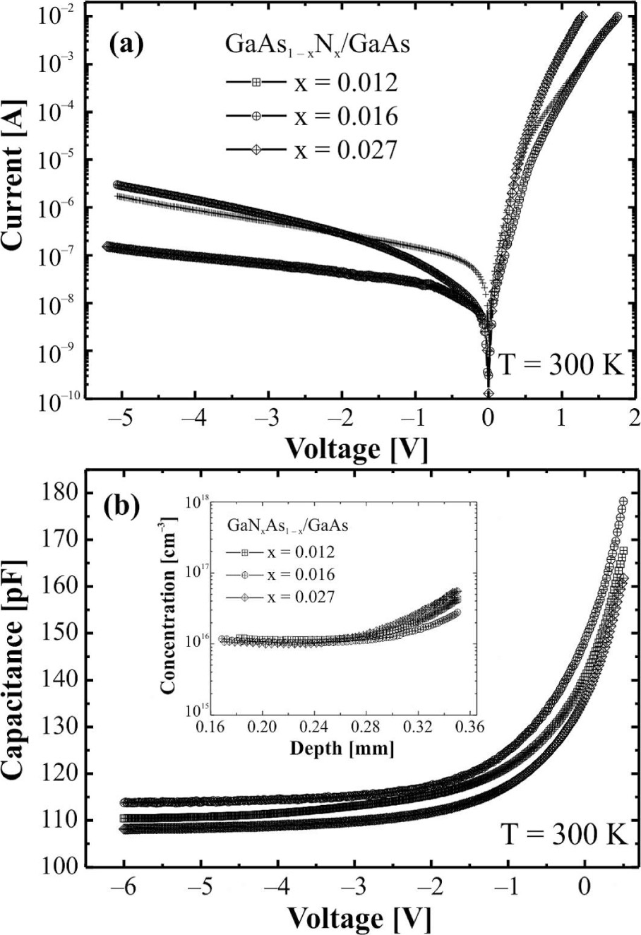
(a) Current-voltage and (b) capacitance-voltage characteristics recorded at 300 K for all studied samples. In the inset of (b) background doping concentration vs. depth profiles are plotted.
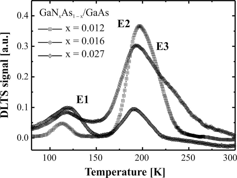
Low-temperature DLTS spectra obtained for the GaNxAs1−x/GaAs heterostructures with different nitrogen contents (x) at a reverse bias voltage (VR) of −2 V, a filling pulse voltage (VP) of 0 V, an emission rate window (en) of 20 s−1, and a filling pulse width (tp) of 50 s.
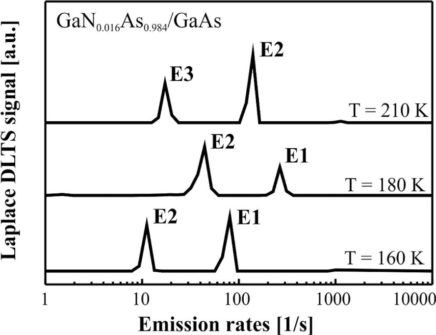
Exemplary Laplace DLTS spectra of the GaN0.016As0.984/GaAs structure, taken at 160 K, 180 K and 210 K for similar experimental conditions as those of conventional DLTS.
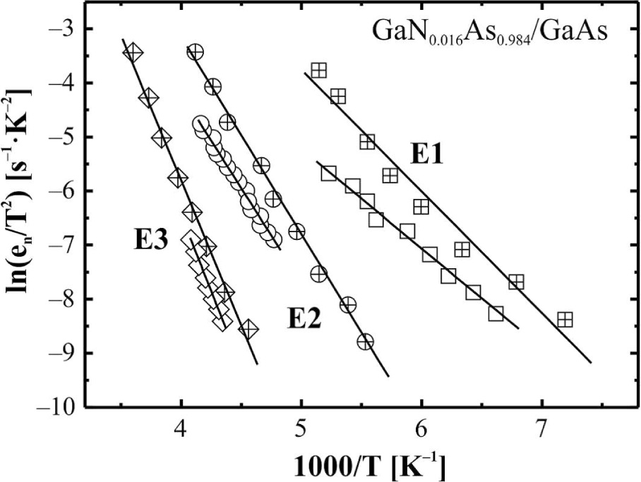
The Arrhenius plots of the peaks E1, E2, E3 depicted in Fig. 2 and Fig. 3 for the GaN0.016As0.984/GaAs structure. Crossed points correspond to conventional DLTS analysis and open points to Laplace DLTS analysis.
Table 1
Activation energies (Ea) and apparent capture cross sections (σa) obtained from conventional DLTS and Laplace DLTS analysis of the traps E1, E2 and E3 observed in GaNxAs1−x/GaAs samples (x = 1.2 % to 2.7 %) in low-temperature spectra (<300 K). In the last column, possible identities of the traps have been made on the basis of comparison with activation energies of the defects observed in as-grown GaAs and GaNAs, as reported in the references given below.
| Trap label | 1.2 % N | GaNAs/GaAs 1.6 % N | 2.7 % N | Possible identity | |||||
|---|---|---|---|---|---|---|---|---|---|
| DLTS | DLTS | LDLTS | DLTS | ||||||
| Ea [eV] | σa [cm2] | Ea [eV] | σa [cm2] | Ea [eV] | σa [m2] | Ea [eV] | σa [cm2] | ||
| E1 | 0.24 | 8.8 × 10⁻¹⁸ | 0.21 | 2.9 × 10⁻¹⁸ | 0.20 | 3.4 × 10⁻¹⁸ | 0.15 | 2.1 × 10⁻¹⁸ | N-relateda−d |
| E2 | 0.32 | 1.7 × 10⁻¹⁶ | 0.32 | 2.5 × 10⁻¹⁶ | 0.30 | 6.6 × 10⁻¹⁶ | 0.32 | 1.6 × 10⁻¹⁶ | EL6e−g |
| E3 | 0.49 | 3.9 × 10⁻¹³ | 0.49 | 3.2 × 10⁻¹⁴ | 0.48 | 1.5 × 10⁻¹⁴ | 0.49 | 5.2 × 10⁻¹⁴ | EL3f−h |
Table 2
Concentration of the electron traps E1, E2 and E3 obtained from DLTS measurements of the GaNxAs1−x/GaAs samples (x = 1.2 % to 2.7 %).
| GaNAs/GaAs | E1 (N-related) | E2 (EL6) | E3 (EL3) |
|---|---|---|---|
| NT [cm−3] | NT [cm−3] | NT [cm−3] | |
| 1.2 % N | 1.3 × 10¹³ | 2.1 × 10¹³ | 1.1 × 10¹³ |
| 1.6 % N | 1.8 × 10¹³ | 4.5 × 10¹³ | 4.2 × 10¹³ |
| 2.7 % N | 1.6 × 10¹³ | 7.0 × 10¹³ | 4.5 × 10¹³ |
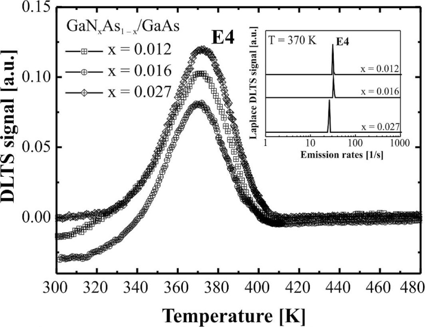
High-temperature DLTS spectra obtained for the GaNxAs1−x/GaAs heterostructures with different nitrogen contents (x). The inset shows corresponding LDLTS spectra recorded at 370 K.
Table 3
Activation energy Ea, apparent capture cross section σa and concentration NT obtained from the conventional DLTS and Laplace DLTS analysis of the trap E4 observed in the GaNxAs1−x/GaAs samples (x = 1.2 % to 2.7 %) in high-temperature spectra (>300 K). In the last column, possible identity of the trap has been proposed.
| GaNAs/GaAs samples | E4 (EL2) | Possible identity | ||||
|---|---|---|---|---|---|---|
| DLTS | LDLTS | |||||
| NT [cm−3] | Ea [eV] | σa [cm2] | Ea [eV] | σa [cm2] | ||
| 1.2% N | 2.3 × 10¹³ | 0.81 | 2.4 × 10⁻¹⁴ | 0.81 | 7.7 × 10⁻¹⁴ | EL2a–c |
| 1.6 % N | 2.0 × 10¹³ | 0.80 | 1.2 × 10⁻¹⁴ | 0.80 | 3.8 × 10⁻¹⁴ | |
| 2.7 % N | 2.6 × 10¹³ | 0.81 | 1.9 × 10⁻¹⁴ | 0.80 | 2.3 × 10⁻¹⁴ | |
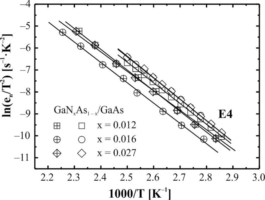
The Arrhenius plots of the peak E4 for all studied samples. Crossed points correspond to conventional DLTS analysis and open points to Laplace DLTS analysis.