
The design of digital systems is significantly influenced by computational speed and the power consumption of the employed logic circuits [1]. Improvements in design predominantly focus on these parameters, with particular emphasis on minimizing power consumption and preventing information loss [2], which is a critical area of concern [1]. In traditional computing systems, the process of computation is irreversible; this means that once the result is complete, the original data used gets cleared, which increases the energy needed to run the system [3]. Furthermore, it has been proven that every case of lost information in irreversible logic produces kTln2 joules of heat [4]. Some excellent alternative technologies, which consist of low-power and high-speed, including reversible logic [5,6], QCA [7–10], and the atomic silicon dangling band [11–14], can be the best option for previous classic technologies like CMOS and VLSI [15,16]. In the following, Bennett demonstrated that employing reversible calculations rather than irreversible ones results in the avoidance of kTln2 joules of energy expenditure [17].
Reversible logical processes cannot lead to data destruction or heat release, hence contributing to the decrease in heat loss [18]. Reversible circuits are constructed through the integration of reversible logic gates [18]. Reversible circuits, often referred to as lossless circuits, exhibit characteristics that prevent both energy loss and information loss [19].
A logic gate is reversible if its input and output combinations are matched one-to-one [20,21]. This implies that each unique input corresponds to a distinct output, so the number of input bits must be the same as the number of output bits [20–23]. Consequently, the input of a reversible gate can be uniquely identified based on its outputs. In reversible logic gates, it is possible to restore input bits even after the output has been generated. Reversible logic gates facilitate the distinction between their inputs and outputs [20–23]. In reversible circuits, the use of fan-out and feedback is prohibited [24,25]. Furthermore, reversible logic is very advantageous in quantum computers due to the intrinsically reversible nature of quantum evolution [19,26].
Furthermore, parity checking functions as a technique for identifying errors in digital logic systems. Reversible circuits that preserve parity utilize reversible logic gates, ensuring that the parity of the input vector corresponds with the parity of the output vector. A reversible circuit preserves parity if its gate is specifically designed for that purpose. Parity-preserving reversible gates facilitate the identification of output faults that affect no more than one logical signal [22,27].
In addition, a quantum computer is conceptualized as a quantum network, or a collection of quantum networks, consisting of quantum logic gates. A single gate includes straightforward procedures performed on qubits, which are two-level quantum systems. Like the classic bits 0 and 1, qubits are the base of quantum information. All unitary operations exhibit reversibility, necessitating that quantum networks be constructed from reversible logical components [28].
The following provides a summary of the literature review. Utilizing existing DFG, IG, and NFT gates, Shams and Haghparast constructed a 2×2 Vedic multiplier that effectively preserved parity and assured reversibility [29].
PourAliAkbar and colleagues introduced three novel reversible blocks, designated as B1, B2, and B3, characterized by a parity-preserving format. Subsequently, utilizing the proposed blocks along with the preexisting gates NFT and DFG, three distinct designs of 2×2 parity-preserving reversible Vedic multipliers were developed. Each design served as a foundation for the creation of larger Vedic multipliers [30].
Ariafar and Mosleh developed a 2×2 Vedic multiplier utilizing the ZCG, FRG, PPTG, and DFG gates, ensuring both reversibility and parity [31].
A reversible block, termed MMM, that maintains parity, was suggested by Rashno et al., and then, a reversible 2×2 Vedic multiplier that maintains parity was developed using the MMM block, along with the existing NFT and E1 blocks [32].
Noorallahzadeh et al. developed three reversible blocks, designated N1, N2, and N3, that ensured parity preservation. Subsequently, they developed a 2×2 Vedic multiplier using N1, N3, and contemporary RF gates to ensure parity preservation [33].
This article examines Vedic multipliers, which are widely utilized in circuit design and related domains due to their superior speed in executing multiplication compared to alternative multiplier types. The Vedic multipliers utilize vertical and cross-multiplication methods to derive the partial product. All of the suggested designs are run using the Qiskit [34] library, both on simulators and on IBM cloud-based quantum processors [35–37].
The substantial contributions of this work are detailed as follows:
Introducing an innovative design of the 5×5 block optimized with minimal implementation costs.
Introducing an innovative design of the 2×2 Vedic multiplier optimized with minimal implementation costs.
Introducing an innovative design of the 2×2 Vedic multiplier optimized with minimal implementation metrics of GO, CNOT-V/V+ count, CI, and GC.
Evaluation and examination of the suggested designs in relation to previous versions.
The organization of the next sections of the paper is as follows: The subsequent part examines the basics of reversible and quantum circuits discussed above. Section 3 discusses the suggested structures in this study. Section 4 encompasses the assessment and discourse on the resultant reversible quantum circuits. The results of the study are ultimately encapsulated in the conclusions presented in Section 5.
This section offers a clear summary of the key concepts associated with reversible and quantum circuits, which are crucial for attaining quantum functionality.
Reversible circuits are described as digital circuits that include an equal quantity of input and output signals. In addition, reversible circuits execute bijections, indicating that each input configuration is associated with a unique output configuration. As a result, calculations can be performed not only from inputs to outputs but also in the reverse direction [24,25].
The key reversible gates that are commonly utilized include NOT gates that reverse the input in the output [22], the Feynman gate is actually called the CNOT gate [38], and the Toffoli gate, which operates with three inputs and three outputs [39].
A Toffoligate, denoted as Tn (k1, k2,…, kn), features n control lines, consisting of (n-1) lines that allow continuous passage through the gate, and its target line inverts the amount for every control line that equals ‘1’. The T1 (k1) is a special structure because it has no control line, and it is called a NOT gate. The T2 (k1, k2) is the notation for the CNOT gate. The T3 (k1, k2, k3) is the most elementary notation for the Toffoli gate [40] (see Figure 1).
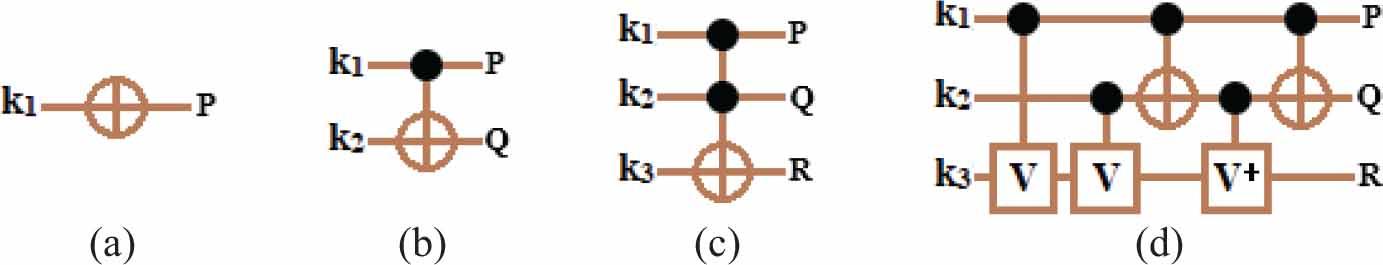
Toffoli gates: (a) T1 (k1), (b) T2 (k1, k2), (c) T3 (k1, k2, k3), (d) quantum layout of T3 (k1, k2, k3).
The following addresses significant metrics utilized for the assessment of reversible quantum circuits (like QC, GC, CI, CNOT-V/V+ count, and GO [22,23,33,41,42]).
Garbage output (GO): Supplementary outputs may be necessary to guarantee the equivalence of inputs and outputs to assure reversibility. Furthermore, unused outputs are acknowledged.
Quantum Cost (QC): refers to the expenditure linked to the circuit, measured as the cost of a basic gate. The calculation relies on the number of basic gates (1×1 and 2×2) required for circuit implementation.
Gate count (GC): refers to the total quantity of gates employed in the implementation of the function.
Constant input (CI): denotes inputs configured to the values 0 or 1, which are essential for sustaining a specific reversible function.
CNOT-V/V+ count: The term denotes the number of gates utilized by the CNOT and Controlled-V/V+ within the circuit design.
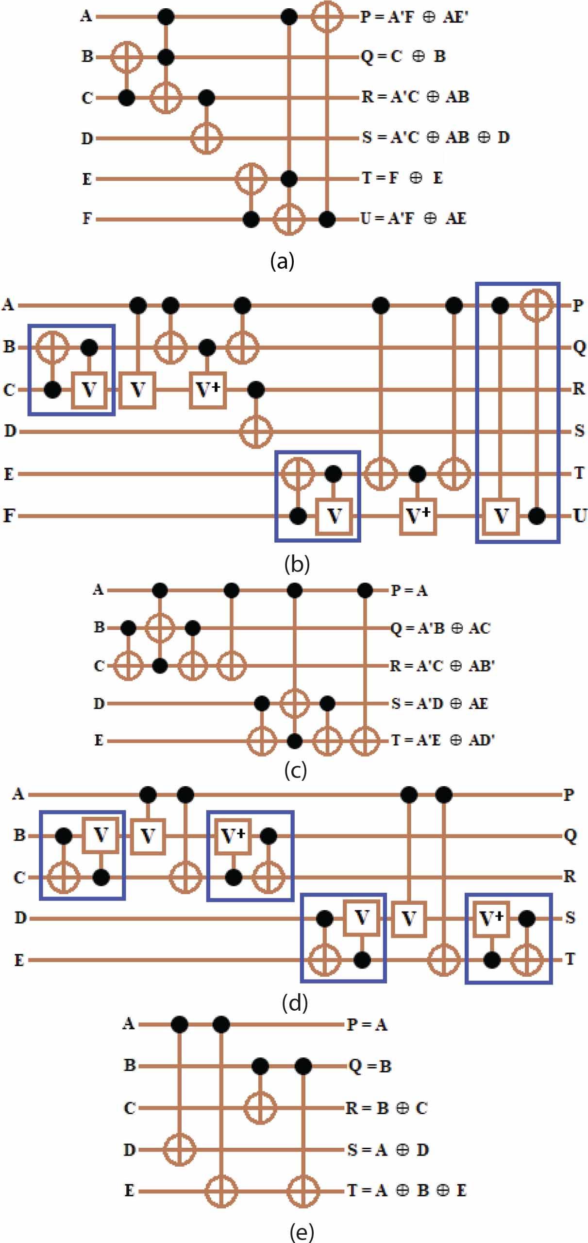
In addition, a reversible logic gate is classified as parity-preserving when the Exclusive-OR of the inputs is equivalent to the Exclusive-OR of the outputs [27]. Several reversible logic gates that maintain parity and are pertinent to the discussion include the L, A, and N2 gates introduced in [22] and [33], respectively. The L [22] is a block that includes 6 inputs and 6 outputs, with a quantum cost quantified as 11, which the Toffoli circuit and its NCV are demonstrated in Figure 2(a-b), respectively, and the A [22] is a block that includes 5 inputs and 5 outputs, with a quantum cost quantified as 8, which the Toffoli circuit and its NCV are illustrated in Figure 2(c) and Figure 2(d), respectively. The N2 [33] is a block that includes 5 inputs and 5 outputs, with a quantum cost quantified as 4, which the Toffoli circuit is illustrated in Figure 2(e).
Quantum computing serves as a potential implementation of reversible logic. The quantum circuits under consideration display characteristics akin to reversible circuits; however, they operate utilizing quantum bits (qubits) rather than classical bits. Qubits are distinct from Boolean logic as they can represent not only the traditional Boolean values of 0 and 1 but also their superposition state. A qubit is characterized as a linear combination of classical Boolean states, positioned within a 2-dimensional complex Hilbert space. In quantum mechanics, the Boolean states 0 and 1 are represented by the two orthonormal states
Every operation on these qubits is represented by a unitary matrix, which is shown with quantum gates. Quantum circuits are constructed using NCV (NOT, CNOT, V, and V+) library gates, whose definitions are illustrated in Figure 3(a-d) [46]:

NCV library.
The NOT gate is a one-qubit operation that transforms the state |0〉 into |1〉 and the state |1〉 into |0〉.
The CNOT gate, sometimes called the XOR quantum gate, operates as a two-qubit gate.
The controlled V gate: A V operation is executed on the target qubit contingent upon the control qubit being in the state of 1. The V operation, referred to as the square root of NOT, is comparable to an inversion when applied twice consecutively. For the controlled V+ gate, a V+ operation is executed on the target qubit contingent upon the control qubit being in the state of 1. The V+ gate executes the opposite function of the V gate, meaning V+ = V−1.
Specifically, these gates modify the target qubit according to the designated unitary matrices
Figure 4(a-c) demonstrates that the cascading of two analogous gates, specifically NOT, controlled-V/V+, and CNOT, yields a buffered outcome without incurring any associated cost [47,48]. Figure 4(d) also shows a kind of quantum gate called the 2-qubit gate. Additionally, running both CNOT and controlled-V operations on the qubits in the arrangement shown in Figure 4(d) results in a total cost of 1 [47,49–51].
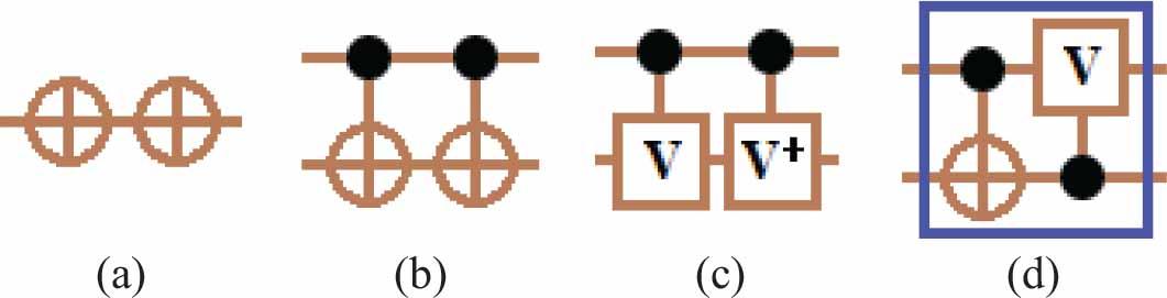
Rules (a) rule 1, (b) rule2, (c) rule3, and (d) integrated 2-qubits.
This section introduces an innovative block designed to preserve parity, then synthesizes it with the transformationbased synthesis technique proposed by Miller et al. [40]. It is a greedy approach since it matches the columns of the truth table by successively putting gates into the circuit, starting from the output. Subsequently, a new 2×2 Vedic multiplier has been developed using the proposed block and existing gates, implemented on the IBM platform.
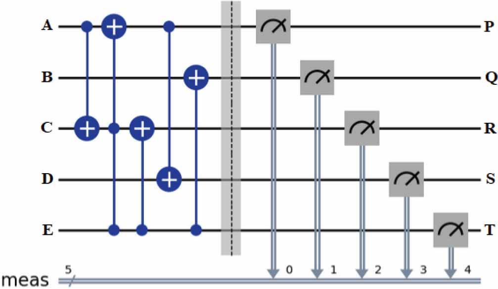
The Q-block functions as a 5×5 block, utilizing inputs A, B, C, D, and E, and producing outputs P, Q, R, S, and T. The outputs are defined by Boolean expressions as presented in Eqs. (1–5):
The Q-block, as specified by Eqs. (1–5) maintains parity preservation.
Verification: To ensure that a functional block is parity-preserving, it is essential that the parities of both the input and output remain identical. The output parity formula is represented as
It is just the same as the parity of the input. Consequently proved.
The Q-block is built by merging the Toffoli gates (T1, T2, and T3), which come from the NCV library, using the transformation-based approach outlined in [40]. Figure 5(a) presents the finalized gate arrangement of the Q-block, which consists of a total of 5 gates. The initial QC measurement of the circuit is 9. Figure 5(b) presents the realization produced with the NCV library, which consists of 9 basic quantum gates. The NCV grid can be further simplified through the application of the integrated and eliminating rules as demonstrated in Figure 4(b) and Figure 4(d). The process results in the optimal layout shown in Figure 5(c), which is defined by a QC of 6.
Suggested Q-block (a) Toffoli layout, (b) NCV layout, (c) optimized NCV layout.
Figure 6 presents an illustration of the proposed Q-block being executed on the IBM platform. Randomly selected states were evaluated within the IBM quantum laboratory, with the corresponding measurement results displayed in Figure 7(a-d). Figure 7(a) shows us that the default simulation (ABCDE=00001) generates the output “01101,” which coincides with the measured output qubits (P, Q, R, S, T). Figure 7(b–d) provides a graph showcasing the qubit measurement findings for different input combinations.
Depicts the proposed Q-block in the IBM platform.
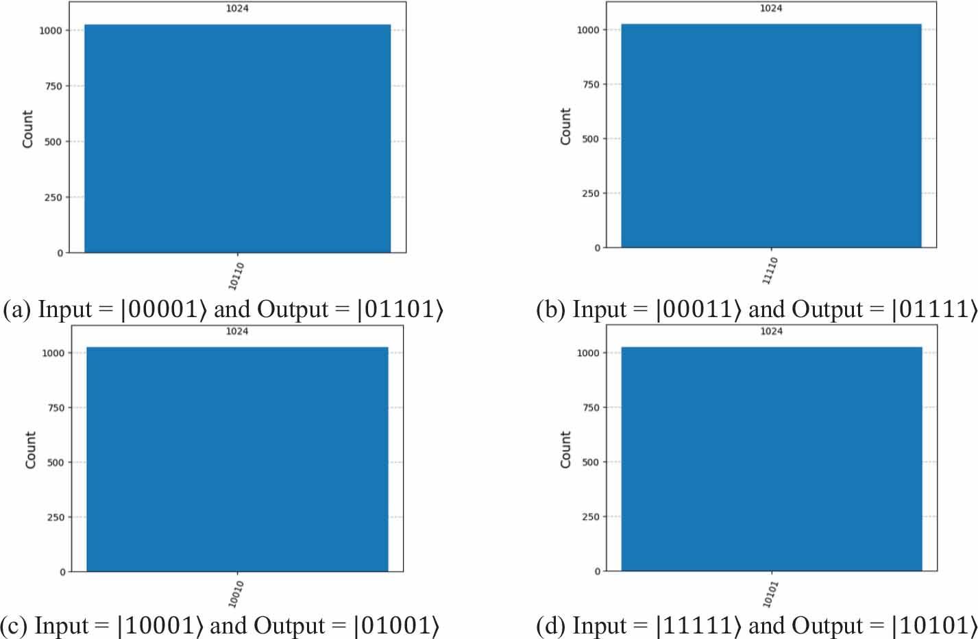
Measurement of Q-block qubits.
The Urdhva Tiryakbhayam (UT) multiplier employs a crosswise multiplication method and is grounded in Vedic techniques [52,53]. Any numerical system, such as binary, decimal, or hexadecimal, can utilize it [31,53]. Multiplication involves two distinct steps. Initially, compute the partial product, followed by the summation of the resultant partial products [53]. The conventional multiplication approach has a significant delay in the computation process as the bit count of the multiplier and multiplicand grows [53]. In the UT approach, the latency of the computation procedure does not escalate proportionally with the additional bits of the multiplier and multiplicand [53].
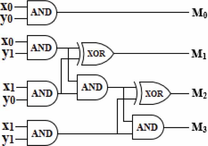
The design of the 2 × 2 Vedic multiplier consists of three distinct stages [53]. The inputs consist of the variables x0, x1, y0, and y1. The outputs are derived from these inputs through the following established relations:
Additionally, the orbital representation of 2×2 Vedic multiplication is demonstrated in Figure 8.
Orbital representation of 2×2 Vedic multiplier [54].
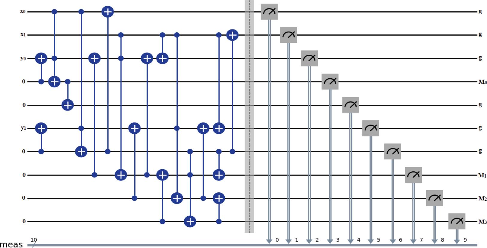
Figures 9 and 10 demonstrate the Toffoli and NCV representations, respectively, of the suggested reversible quantum Vedic multiplier, which consists of blocks A, L, and Q.
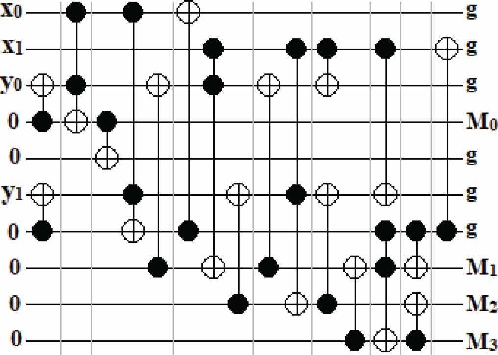
Toffoli layout of the proposed 2×2 Vedic multiplier.
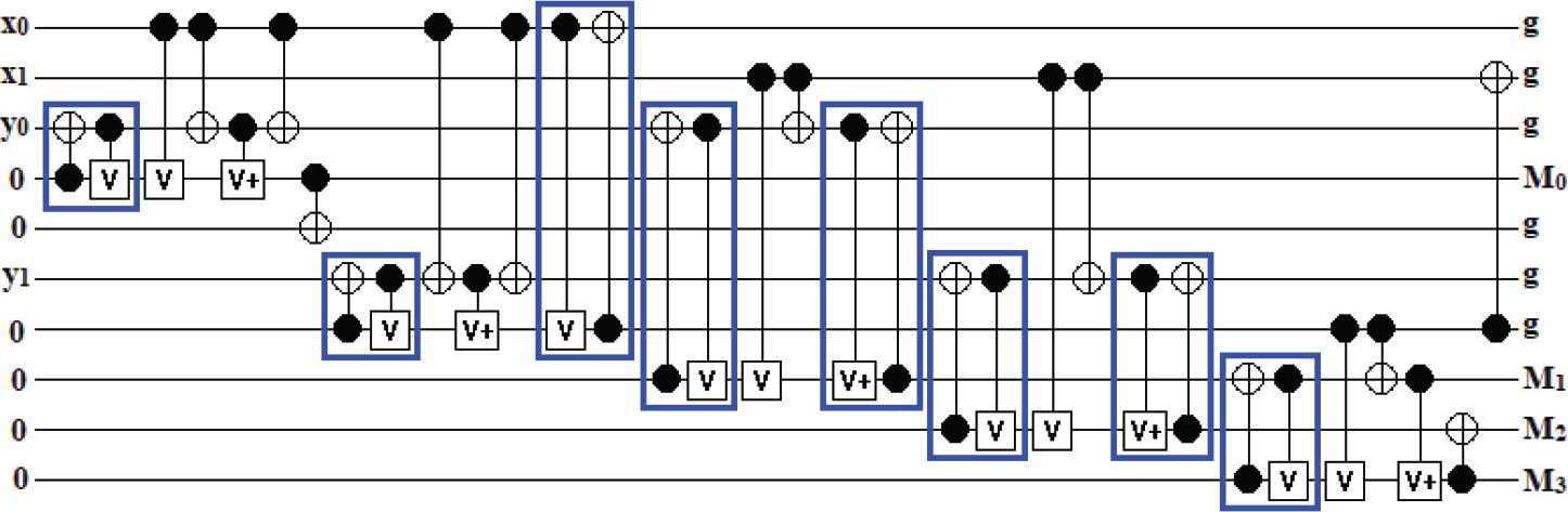
NCV layout of the proposed 2×2 Vedic multiplier.
The GO, GC, and CI metrics show the 6, 3, and 6 values for the suggested Vedic multiplier, respectively. Moreover, the overall QC of the suggested 2×2 Vedic multiplier is assessed as follows:
Figure 11 demonstrates the execution of the suggested 2×2 Vedic multiplier on the IBM system. Figure 12(a-d) shows the measurement results from the IBM quantum laboratory for different randomly chosen states. Figure 12(a) depicts that the default simulation (a0a1b0b1 = 0000) has an output “0000,” which corresponds to measured output qubits (M0, M1, M2, and M3). Figure 12(b-f) shows a plot for illustrative purposes of the qubit measurement results for different inputs.
Depicts the proposed 2×2 Vedic multiplier in the IBM platform.
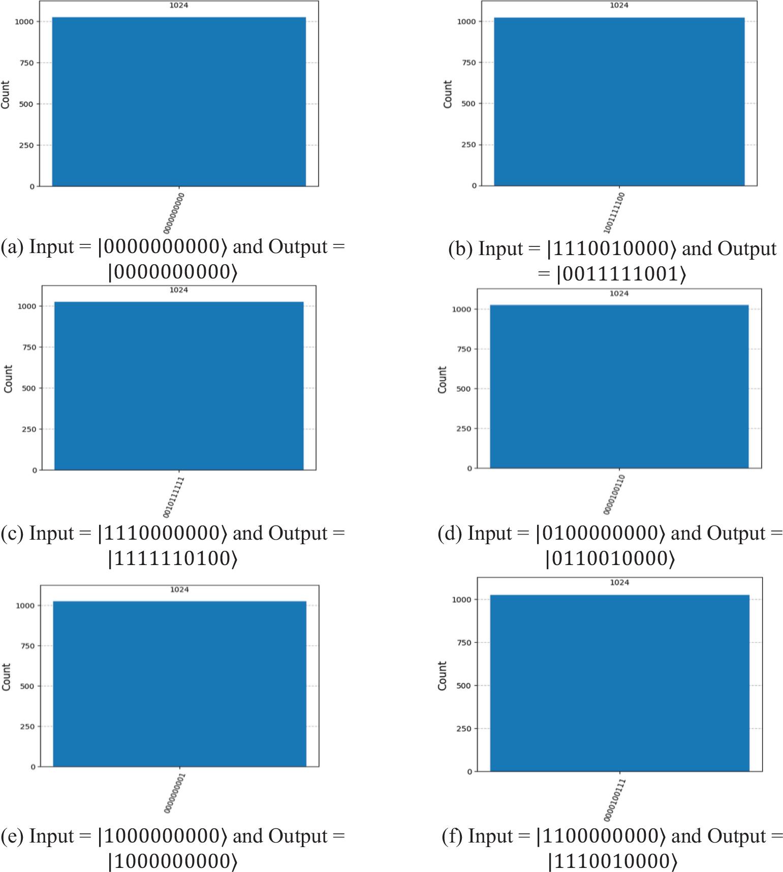
Measurement process of qubits in a 2×2 Vedic multiplier configuration.
Besides, constructing a 4-bit Vedic multiplier requires 2×2 Vedic multipliers and RCA adders [33]. In the proposed design, we employed the 4-bit RCA adder described in [33], as illustrated in Figure 13.
Circuit View of 4-bit RCA presented in [33].
The proposed 4-bit Vedic multiplier, designed using three RCA adders, four 2×2 Vedic multipliers, and four N2-blocks, is shown in Figure 14.
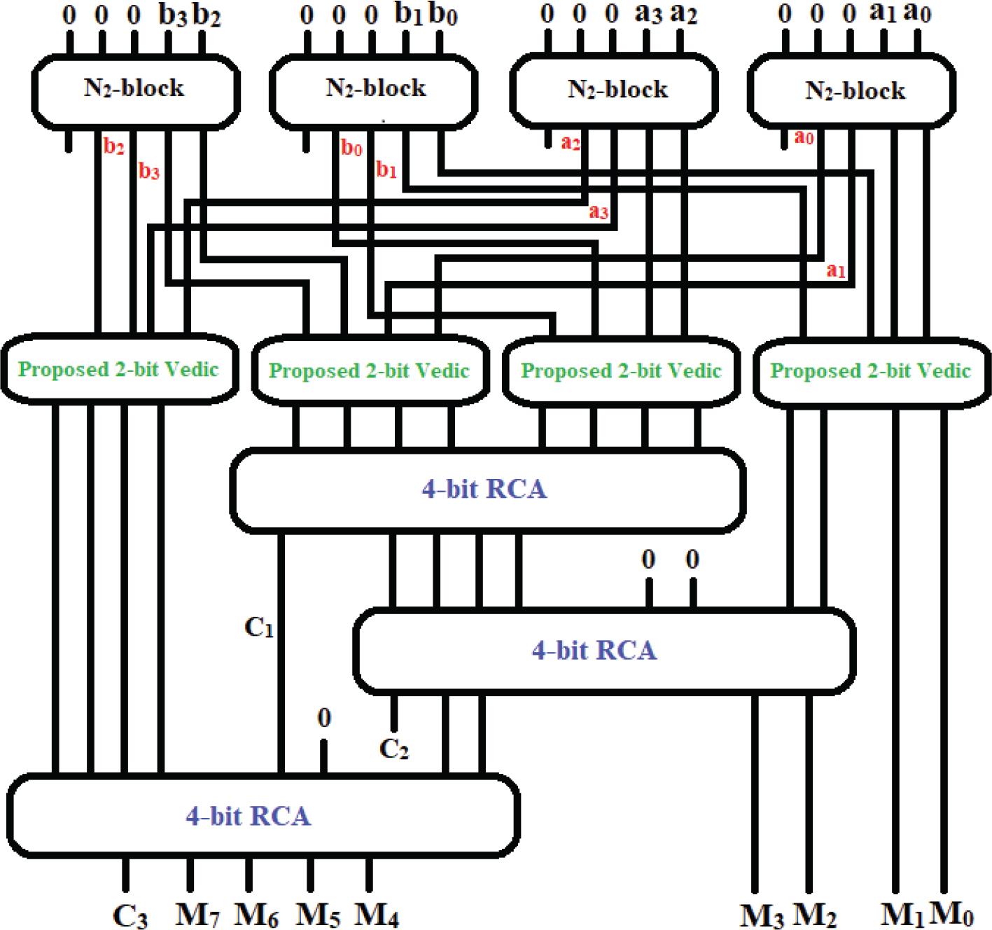
Proposed 4-bit Vedic multiplier.
The GO, GC, and CI metrics for the proposed 4-bit Vedic multiplier are 61, 28, and 60, respectively. Furthermore, the overall QC of the proposed 4-bit Vedic multiplier is evaluated as follows:
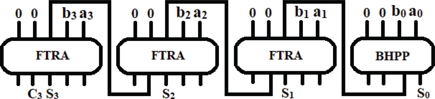
In addition, the proposed 8-bit and 16-bit RCAs, designed using the BHPP block [55] and the FTRA gate [56], are shown in Figure 15(a–b).
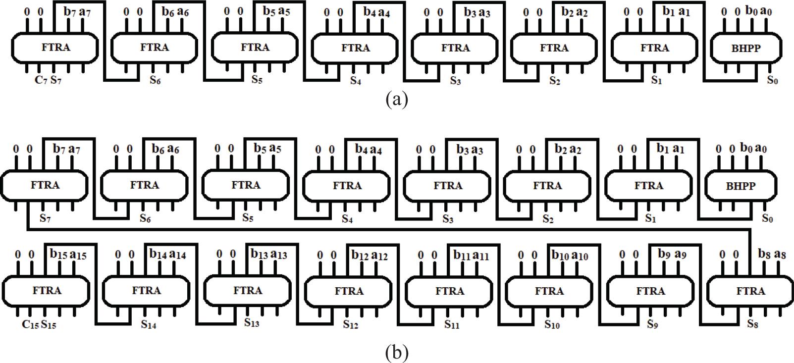
Proposed RCA (a) 8-bit and (b) 16-bit.
The GO, GC, and CI metrics show the 23, 8, and 16, and 47, 16, and 32 values for the suggested 8-bit RCA and 16-bit RCA, respectively. Moreover, the overall QC of the suggested 8-bit RCA and 16-bit RCA is assessed as follows:
Furthermore, the proposed 8-bit and 16-bit Vedic multipliers, designed using RCA adders (8-bit and 16-bit), Vedic multipliers (4-bit and 8-bit), and N2-blocks, are shown in Figure 16 and Figure 17.
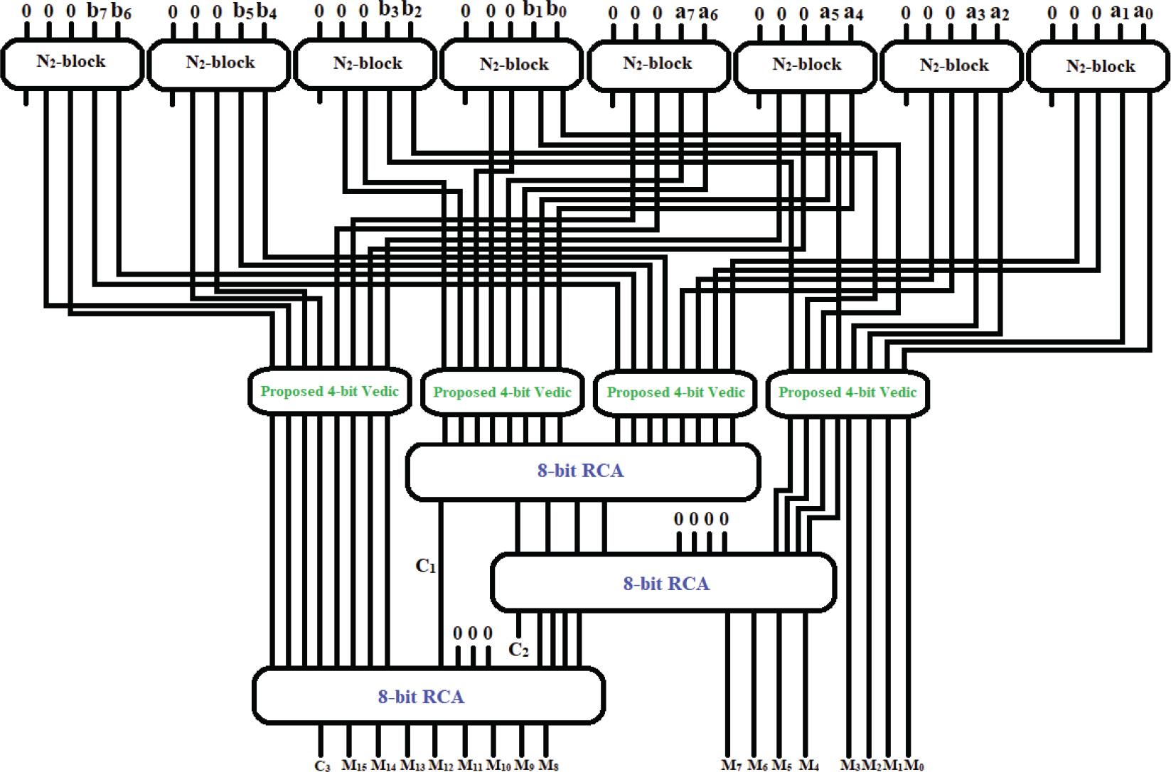
Proposed 8-bit Vedic multiplier.
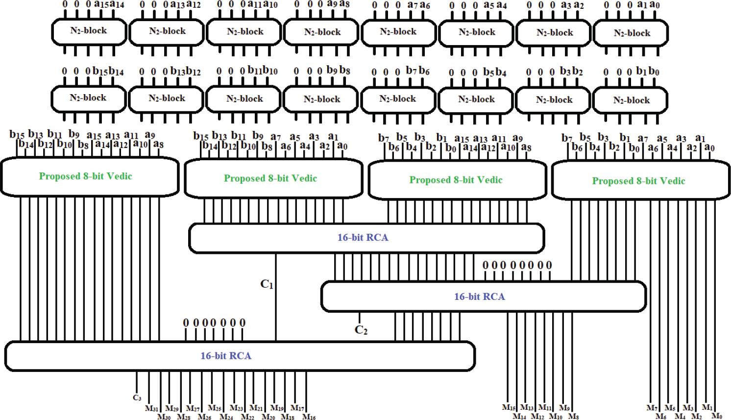
Proposed 16-bit Vedic multiplier.
The GO, GC, and CI metrics for the proposed 8-bit Vedic multiplier are 321, 144, and 312, respectively. Furthermore, the overall QC of the proposed 8-bit Vedic multiplier is evaluated as follows:
For the proposed 16-bit Vedic multiplier, the GO, GC, and CI metrics attain values of 1441, 640, and 1392, respectively. In addition, the overall QC is determined as follows:
This section evaluates the implementation of the proposed reversible quantum systems and contrasts them with current works documented in the literature. Table 1 lists important specifications regarding the Vedic multiplier circuits. The table includes comprehensive information, such as the CI, CNOT-V/V+ count, GO, GC, and QC.
A comparison of various 2×2 Vedic multipliers.
| Designs | CI | QC | GC | GO | CNOT-V/V+ count |
|---|---|---|---|---|---|
| In [29] | 16 | 42 | 10 | 16 | 50 |
| In [30]#1 | 16 | 40 | 10 | 16 | 50 |
| In [30]#2 | 10 | 34 | 7 | 10 | 44 |
| In [30]#3 | 9 | 31 | 7 | 9 | 39 |
| In [31] | 8 | 30 | 6 | 8 | 37 |
| In [32] | 8 | 29 | 5 | 8 | 37 |
| In [33] | 7 | 27 | 5 | 7 | 35 |
| Proposed | 6 | 25 | 3 | 6 | 33 |
| imp% in [29] | 62.50 | 40.47 | 70.00 | 62.50 | 34.00 |
| imp% in [30]#1 | 62.50 | 37.50 | 70.00 | 62.50 | 34.00 |
| imp% in [30]#2 | 40.00 | 26.47 | 57.14 | 40.00 | 25.00 |
| imp% in [30]#3 | 33.33 | 19.35 | 57.14 | 33.33 | 15.38 |
| imp% in [31] | 25.00 | 16.66 | 50.00 | 25.00 | 10.81 |
| imp% in [32] | 25.00 | 13.79 | 40.00 | 25.00 | 10.81 |
| imp% in [33] | 14.28 | 7.40 | 40.00 | 14.28 | 5.71 |
| Average saving | 37.51 | 23.09 | 54.89 | 37.51 | 19.38 |
The findings presented in Table 1 indicate that the suggested 2×2 Vedic multiplier has enhanced performance regarding QC. The efficiency metrics indicating CNOT-V/V+ count, GC, GO, and CI demonstrate that the architecture exceeds that of its predecessors. Table 1 clearly shows the subsequent details:
The proposed scheme has only 3 gates, which deliver better outcomes than the previous methods [33] and [32] using 5 gates. Furthermore, it demonstrates a 40% improvement compared to the leading studies in [33] and [32].
The proposed scheme has only 6 CI, and delivers better outcomes than the previous method [33] using 7 CI. Furthermore, it demonstrates a 14.28% improvement compared to the leading study in [33].
The proposed scheme has only 6 GO that deliver better outcomes than the previous method [33] using 7 GO. Furthermore, it demonstrates a 14.28% improvement compared to the leading study in [33].
The proposed scheme has only 25 QC and delivers better outcomes than the previous method [33] using 27 QC. Furthermore, it demonstrates a 7.40% improvement compared to the leading study in [33].
Our proposed scheme has only 33 CNOT-V/V+ count, and delivers better outcomes than the previous method [33] using 35 CNOT-V/V+count. Furthermore, it demonstrates a 5.71% improvement compared to the leading study in [33].
In addition, the proposed design yields average savings of 19.38%, 37.51%, 37.51%, 23.09%, and 54.89% for CNOT-V/V+ count, GO, CI, QC, and GC, respectively. Additionally, the graphical view of the improvement associated with the suggested design is illustrated in Figure 18.
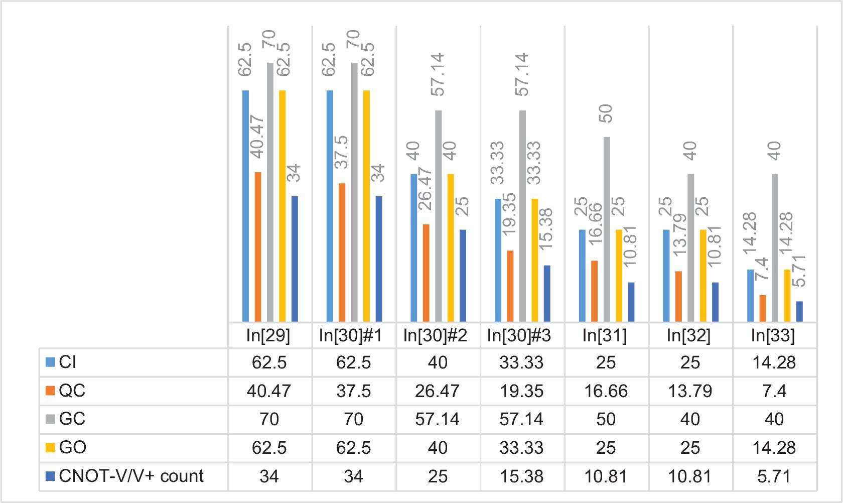
Graphical view of the suggested design enhancement.
This study introduced a distinctive block, noted for its low quantum cost and overall cost-effectiveness. Afterwards, a parity-preserving reversible quantum 2×2 Vedic multiplier with low quantum cost was presented using the suggested block and prior gates. Moreover, extended designs of Vedic multipliers with 4-bit, 8-bit, and 16-bit configurations were presented. This study’s design demonstrated notable enhancements compared to earlier designs, particularly regarding QC, CI, GO, GC, and CNOT-V/V+ count. The research findings indicated that the savings realized in QC, GC, CI, CNOT-V/V+, and GO were 23.09%, 54.89%, 37.51%, 19.38%, and 37.51%, respectively. In future work, the Vedic multiplier has potential uses in particular application areas, particularly integration with quantum processor architectures. Its performance is described as substantially boosting the ability of quantum computing. In addition, examining the possible uses in the area of high-performance computing, in machine learning algorithms, and in real-time systems will be very beneficial.