
Fig. 1.
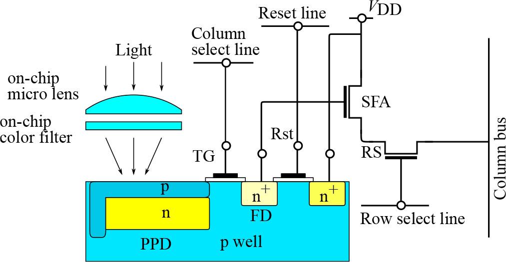
Fig. 2.
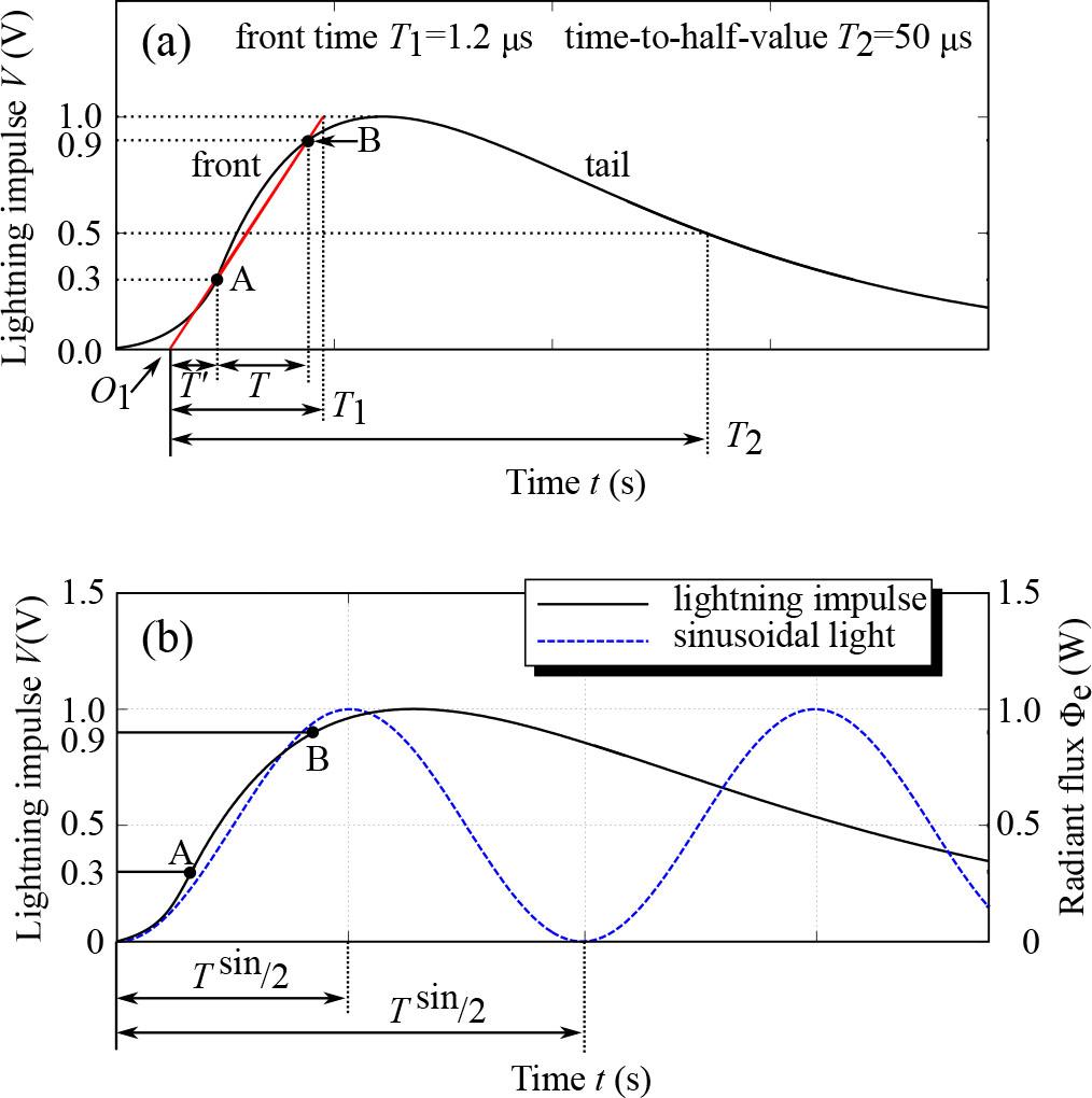
Fig. 3.
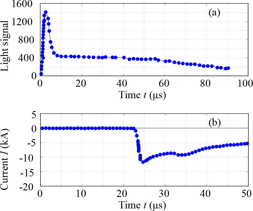
Fig. 4.
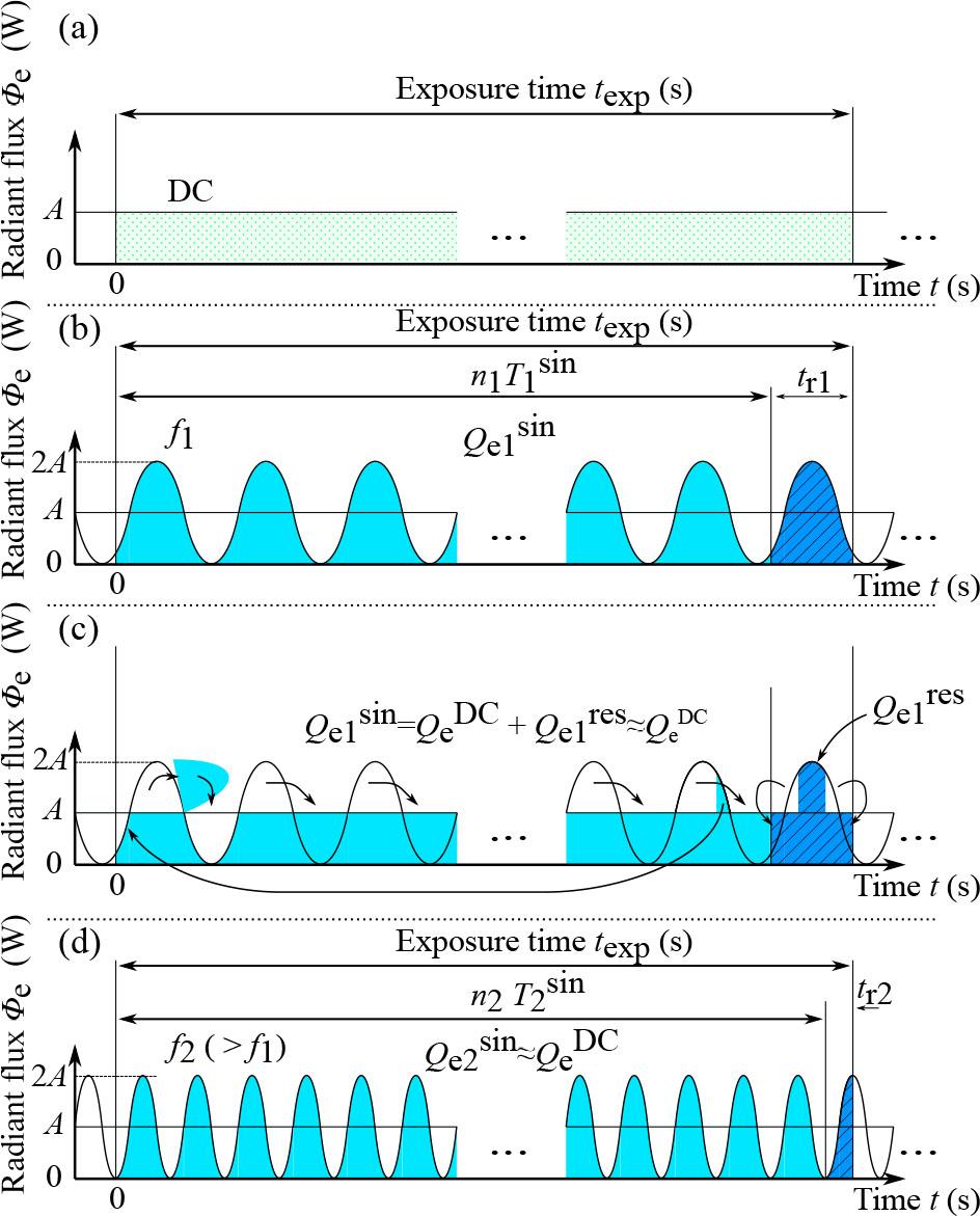
Fig. 5.
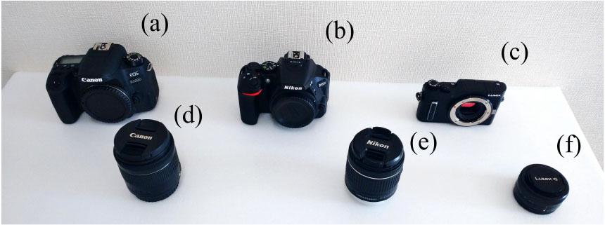
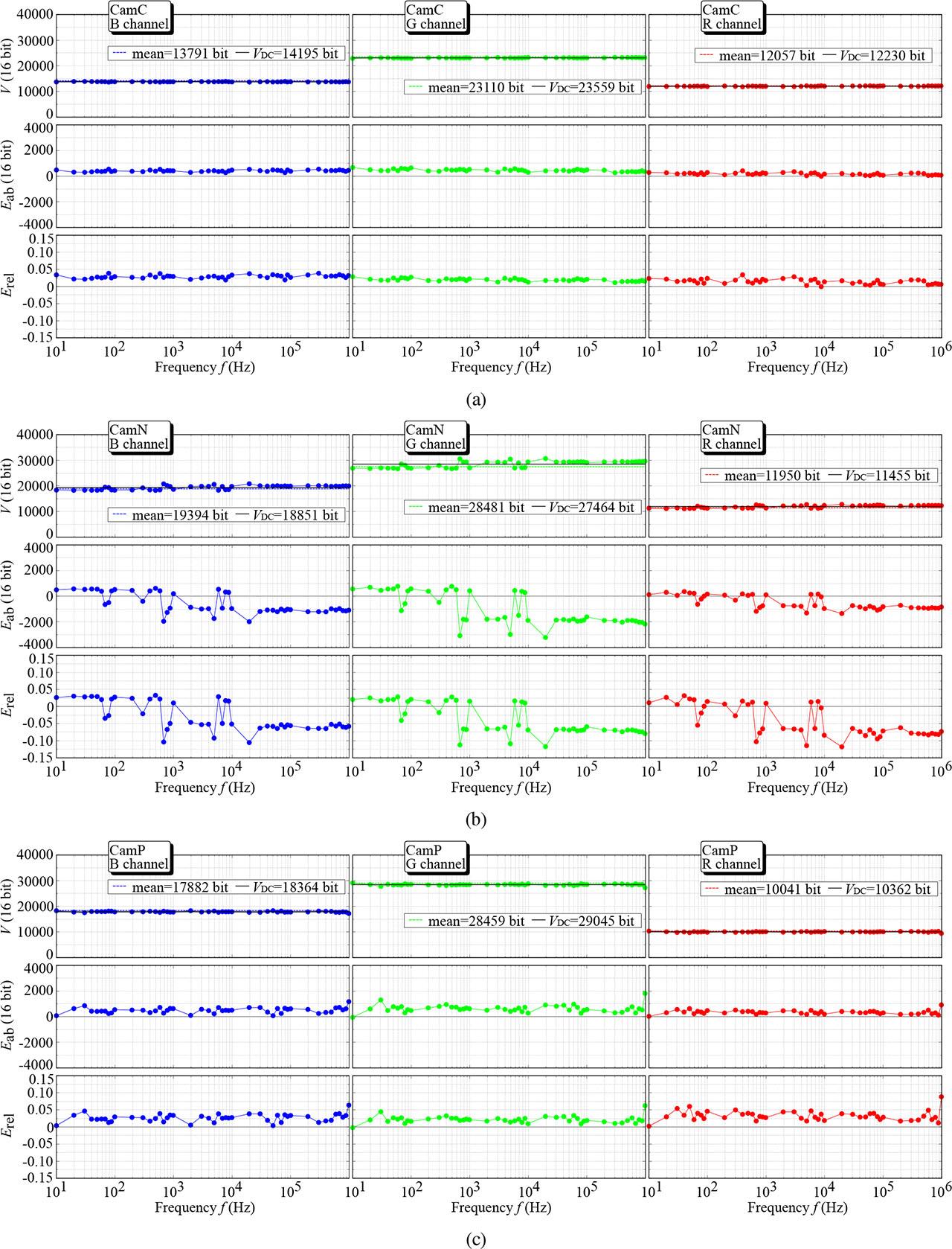
Fig. 6.
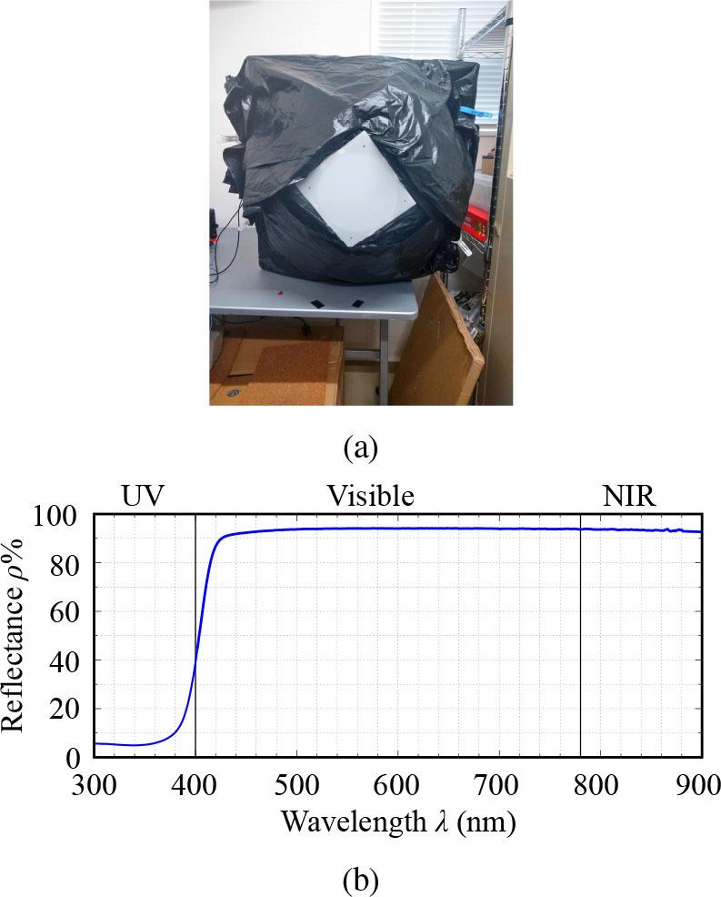
Fig. 7.
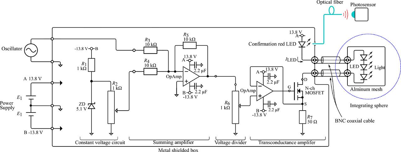
Fig. 8.
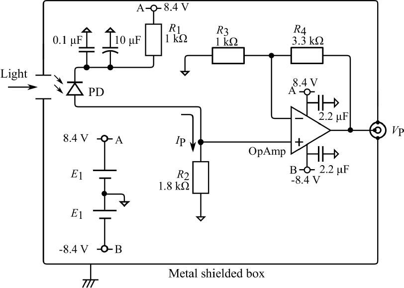
Fig. 9.
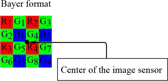
Fig. 10.
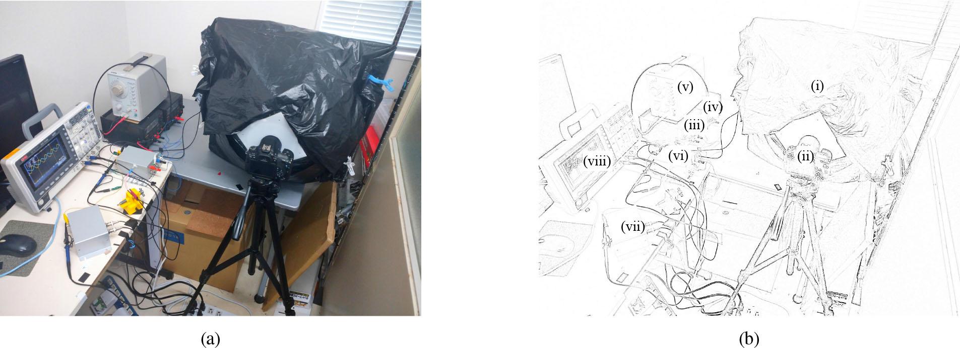
Fig. 11.
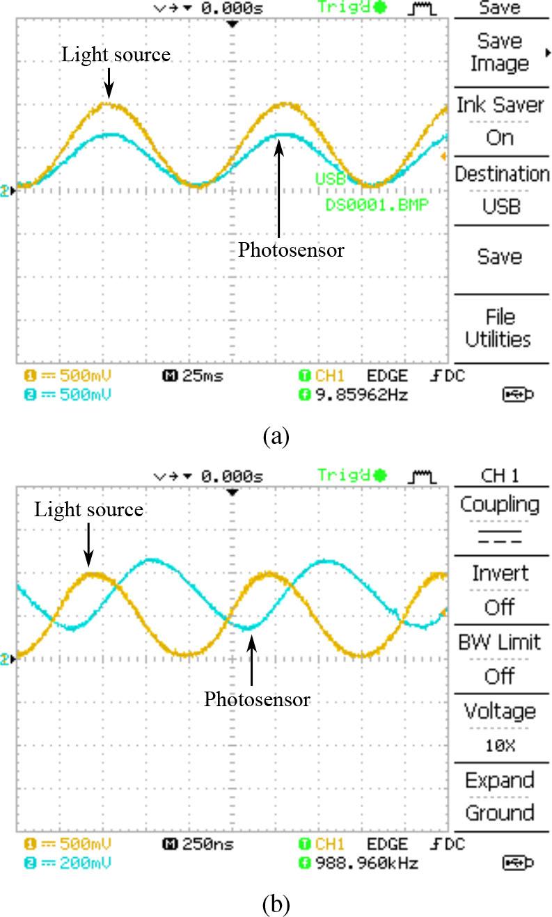
Fig. 12.
Cameras and lenses used, along with their corresponding symbols_ In subsequent sections, each camera and lens is represented by the symbols listed in the Symbol column_
| Camera/Lens | Manufacturer | Product name | Symbol |
|---|---|---|---|
| Camera | Canon | EOS 9000D | CamC |
| Camera | Nikon | D5600 | CamN |
| Camera | Panasonic | Lumix DC-GF10W | CamP |
| Lens | Canon | EF-S18-55mm F4-5.6 IS STM | Cf18-55 |
| Lens | Nikon | AF-P DX NIKKOR 18-55mm f/3.5-5.6G VR | Nf18-55 |
| Lens | Panasonic | Lumix G VARIO 12-32mm/F3.5-5.6 ASPH./MEGA O.I.S. | Pf12-32 |
Dark values of the image sensors in three cameras_
| Camera | B | G | R |
|---|---|---|---|
| CamC | 2045.90 | 2045.28 | 2045.72 |
| CamN | 2408.16 | 2406.07 | 2408.68 |
| CamP | 2288.0 | 2282.0 | 2284.0 |
Electronic components in the LED driver and photosensor_ The physical quantities listed include: bias current and slew rate of the operational amplifier (IB and SR), rise and fall times of the MOSFET (tr and tf), zener voltage (VZ), luminous intensity (IV), forward current of the LED (IF), photocurrent of the photodiode (IP), and illuminance (EV)_
| Circuit | Part symbol | Part name | Manufacturer | Product number | Description |
|---|---|---|---|---|---|
| LED driver | OpAmp | Operational amplifier | Nisshinbo Micro Devices | NJM2742D | IB = 80 nA, SR= 10 μs |
| LED driver | N-ch MOSFET | MOSFET | Microchip Technology | DN2540N3-G | tr = 15 ns, tf = 20 ns |
| LED driver | ZD | Zener diode | Nexperia | BZX79-C5V1,113 | VZ = 5.1 V |
| LED driver | LED | White LED | Cree LED | C503D-WAN-CCbEb151 | Iv = 40 cd, IF = 20 mA |
| LED driver | Red LED | Red LED | DiCUNO | – | Red, Iv = 3 cd, IF = 20 mA |
| LED driver | Coaxial cable | Coaxial cable | – | RG174 | BNC terminated, 1.5 m, 50 Ω |
| Photosensor | OpAmp | Operational amplifier | Nisshinbo Micro Devices | NJM072BD (discontinued) | IB = 13 pA, SR = 13 μs |
| Photosensor | PD | Photodiode | ams-OSRAM | BPW 34 | IP ≥ 55 μA, EV = 1000 lx |
| Photosensor | E1 | Ni-MH rechargeable battery | RS Pro | 199-646 | 8.4 V, capacity 200 mAh |
Camera settings for photography_ Brightness information is influenced by the exposure time t, ISO gain, focal length f, and F-number F/#_ The exposure time and ISO gain are directly related to the image sensors, while the focal length and F-number pertain to the lenses used_
| Combination | Camera | Lens | ||
|---|---|---|---|---|
| Camera-Lens | t (s) | ISO | f (mm) | F/# |
| CamC-Cf18-55 | 1 | 100 | 18 | 4 |
| CamN-NCf18-55 | 1 | 100 | 18 | 4 |
| CamP-Pf12-32 | 1/2 | 200 | 13 | 4 |