
Since the introduction of the complementary metal-oxide-semiconductor (CMOS) image sensor in 1993 [1], its performance has significantly advanced, with pixel sizes now reaching approximately 1 μm or less (e.g., Fig. 7.3 in [2]). Digital cameras equipped with CMOS image sensors have become widespread, and although consumer-grade models are relatively affordable, their performance remains impressive. The ability to use these consumer-grade digital cameras as scientific measuring tools would be highly beneficial across various academic fields. Indeed, several studies have already employed consumer-grade digital cameras to study phenomena such as lightning (e.g., [3,4,5,6,7,8,9]), electrical discharges (e.g., [10]), sky photometry (e.g., [11,12,13]), and aurora borealis (e.g., [14,15,16]). Additionally, the relationship between the brightness of an object and camera settings has been explored [17].
In brightness analysis, some objects exhibit almost no change in brightness over time, while others exhibit rapid, significant fluctuations. Objects with extremely rapid brightness changes include lightning [18,19,20] in atmospheric electricity, spark discharges in electrical engineering, periodic variable auroras in planetary physics, and transient astronomical objects in time-domain astronomy, among others. This study focuses specifically on these phenomena. Lightning discharges are brief events, with their light intensity peaking within 0.5–1 μs [21]. In electrical engineering, lightning impulse voltage and switching impulse voltage are utilized to analyze spark discharges and assess the performance of power equipment (e.g., [10, 22]). The front times for lightning impulse voltage and switching impulse voltage are 1.2 μs and 250 μs, respectively. Experimental studies of arc discharges have reported luminosity front times of approximately 2–3 μs (e.g., Table 1 in [10]). In planetary physics, pulsating auroras, with brightness change periods ranging from 2 to 20 s, and flickering auroras, with periods of 0.1 to 1 s, are well-documented. In 2012, Kataoka et al. reported a fast-flickering aurora with a period of approximately 0.02 s and a frequency of 45 Hz [23]. While astronomy typically focuses on objects and phenomena with brightness changes over seconds to years, time-domain astronomy specifically investigates objects with brightness variations occurring in less than a second (from milliseconds to seconds) (e.g., Fig. 1, [24]). As demonstrated, numerous fields are increasingly studying objects with extremely rapid brightness fluctuations. Among these examples, the fastest phenomenon is the rise time of lightning, which is approximately 1 μs. If a sinusoidal wave approximates this rise time, its frequency is approximately 500 kHz.
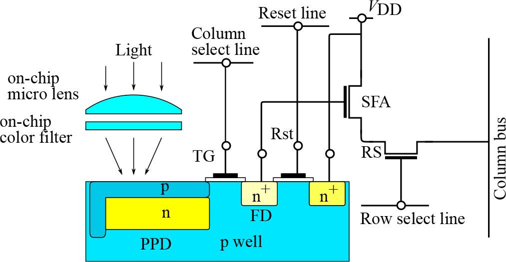
Schematic of a single four-transistor pixel in a CMOS image sensor based on an active pixel sensor design. The pixel includes a pinned photodiode (PPD), a transfer gate (TG), a floating diffusion (FD), a reset transistor (Rst), a source follower amplifier (SFA), and a row select transistor (RS). An on-chip microlens and an on-chip color filter are positioned above the PPD.
Cameras and lenses used, along with their corresponding symbols. In subsequent sections, each camera and lens is represented by the symbols listed in the Symbol column.
| Camera/Lens | Manufacturer | Product name | Symbol |
|---|---|---|---|
| Camera | Canon | EOS 9000D | CamC |
| Camera | Nikon | D5600 | CamN |
| Camera | Panasonic | Lumix DC-GF10W | CamP |
| Lens | Canon | EF-S18-55mm F4-5.6 IS STM | Cf18-55 |
| Lens | Nikon | AF-P DX NIKKOR 18-55mm f/3.5-5.6G VR | Nf18-55 |
| Lens | Panasonic | Lumix G VARIO 12-32mm/F3.5-5.6 ASPH./MEGA O.I.S. | Pf12-32 |
The key issue is whether the image sensor of a digital camera can accurately capture objects with rapid brightness fluctuations. Silicon-based photodiodes, commonly used in image sensors, have rise and fall times ranging from several nanoseconds to tens of nanoseconds. The characteristics of photodiodes in image sensors are highly influenced by the manufacturer’s design parameters, such as impurity concentration and the layer thickness of the P-type, N-type, and depletion regions. However, these design parameters are often proprietary and not accessible to end users. It has been reported that the lifetime of minority carriers depends on carrier concentration, decreasing as the concentration increases [25,26,27]. When light is incident on the photodiode for a short duration, the carrier lifetime is expected to be shorter, depending on the concentration. Furthermore, the time required for carriers generated outside the depletion region to reach it via diffusion is relatively long, on the order of a few microseconds. As carrier concentration increases, the carrier lifetime shortens—from a few microseconds to several tens of microseconds—raising the likelihood of carrier loss through recombination.
Given these factors, it remains uncertain whether the carriers generated by the photodiode in large quantities during brief time intervals are effectively captured as electrical signals. Thus, the only way to determine whether an image sensor can correctly capture bright light with fast luminance changes is through experimental verification. To date, to the best of our knowledge, no such studies have been conducted, making the development of a novel method to analyze the photoresponse of image sensors to rapid luminance changes highly valuable. This study seeks to clarify the photoresponse of image sensors to abrupt changes in light intensity, as described above. Since it is highly challenging to analyze image sensor signals within a few hundred microseconds, we have developed a method to assess whether luminance is accurately captured by integrating over time, rather than relying on short-time signal analysis.
In this study, we theoretically developed a method for analyzing the photoresponse of image sensors to rapid light fluctuations. To validate this analytical approach, we designed a light source capable of emitting sinusoidal light over a frequency range from DC to 1 MHz, along with a photosensor capable of detecting rapid changes in light within this range. Using the developed light source and photosensor, we irradiated the image sensors of three consumer-grade digital cameras with sinusoidal light of constant amplitude at frequencies below 1 MHz and experimentally analyzed the resulting pixel values.
Theoretically, if the amplitude of the sinusoidal wave remains constant and the image sensor correctly captures the light, the pixel values should remain unchanged regardless of frequency. The experimental results showed that the pixel values of the three consumer-grade cameras remained nearly constant across sinusoidal light frequencies from DC to 1 MHz. This indicates that the image sensors of the three cameras accurately captured sinusoidal light up to 1 MHz, confirming the validity of the analytical method we developed. Furthermore, this suggests that when using the three cameras analyzed in this study to capture fast phenomena such as lightning, the light from such events can be accurately recorded. The findings of this study offer valuable contributions to various fields that rely on photometry.
Fig. 1 illustrates a schematic of a single pixel in a CMOS color image sensor. When light reaches a pixel, it passes through an on-chip microlens and an on-chip color filter before being converted from photons to electrons by the pinned photodiode (PPD). The electrons generated by photoelectric conversion in the PPD travel through the transfer gate (TG) and are stored in the floating diffusion (FD). In the FD, a voltage signal is generated from the stored charges via charge-to-voltage conversion, which then flows through the source follower amplifier (SFA) to the signal bus.
The key question is whether the image sensor can accurately capture rapid brightness changes. From the perspective of the image sensor, this issue is further complicated by the following factors:
Did the PPD perform photoelectric conversion correctly?
Did the charge generated by the PPD pass through the TG correctly?
Did the charge-to-voltage conversion occur properly in the FD?
Did the voltage signal pass correctly through the SFA and signal bus?
Upon reaching the analog front end, was the voltage signal correctly converted into RAW data?
This study specifically focuses on (1). While factors (2) to (5) are generally not problematic in low-speed photography, they become significant concerns in high-speed photography. In such cases, conducting high-speed experiments is challenging due to low brightness (i.e., low pixel values) and substantial noise. Furthermore, no camera setting can analyze the rise time of lightning, which is approximately 1 μs. Therefore, (2) to (5) are outside the scope of this study. These factors depend on device design parameters, such as the physical properties of materials and the width of the wiring, which are typically inaccessible to end users. However, (1) can be investigated through time integration. Therefore, we developed an analytical method to examine the photoresponse of image sensors by focusing on (1).
Among the objects and phenomena exhibiting rapid brightness changes, as discussed in Section 1, lightning is one of the fastest known phenomena, with a typical 10/90 rise time of 0.5–1 μs [21]. The next fastest phenomenon is the wavefront of the lightning impulse voltage, which has a rise time of 1.2 μs, as defined in IEC 60060-1. Fig. 2 illustrates the waveform of the lightning impulse voltage alongside the sinusoidal curve approximating the wavefront. For lightning impulse voltage (Fig. 2 (b)), the wavefront with the rise time of T1 = 1.2 μs is approximated by a half period of sinusoidal light, and its period Tsin is obtained as
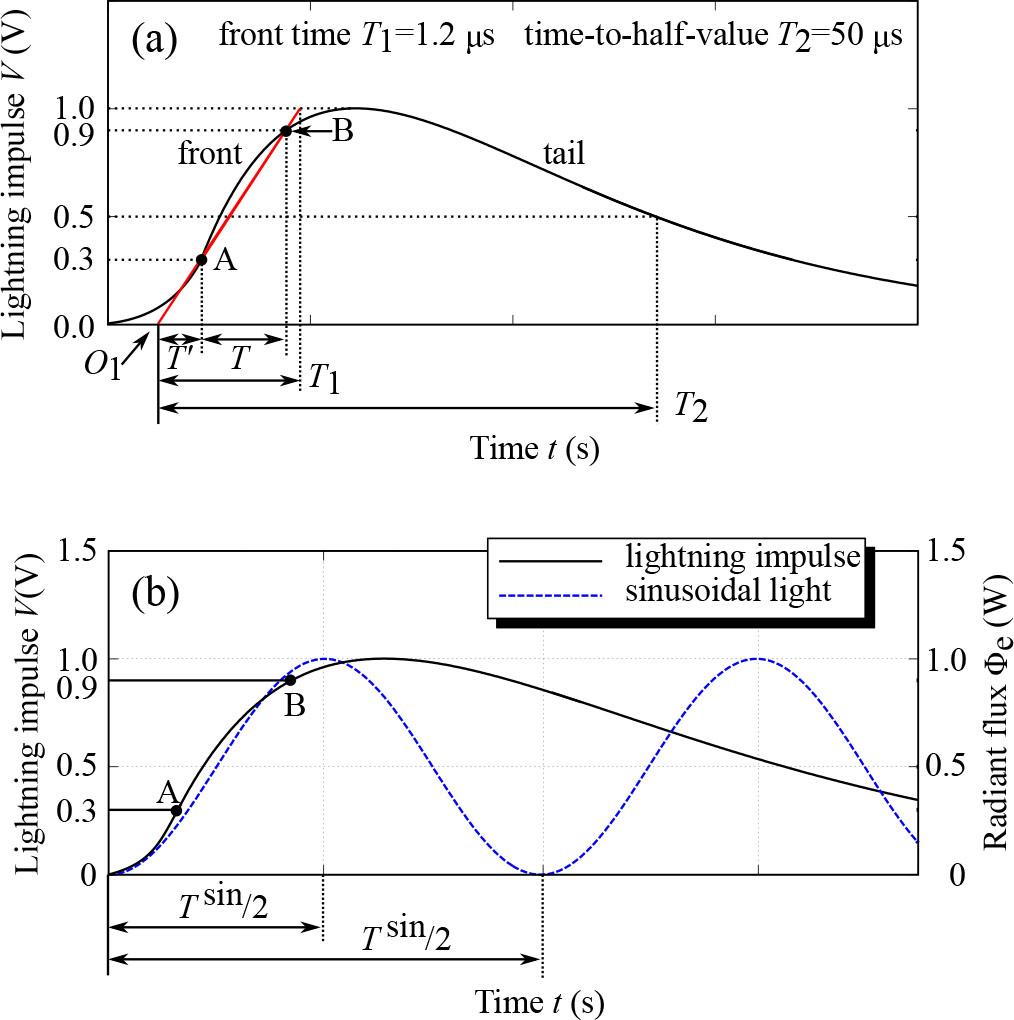
(a) Lightning impulse voltage waveform (e.g., Fig. 2.23, Chapter 2 [28]), and (b) illustration of the wavefront of the lightning impulse voltage (solid line) approximated by sinusoidal light (dashed line) as indicated by the radiant flux Φe. The front time T1 is 1.2 μs, and the time-to-half-value T2 is 50 μs. Both T1 and T2 start from the virtual origin O1. The period of the sinusoidal light is denoted by Tsin. The lightning impulse voltage and radiant flux Φe are normalized, with their maximum values expressed as unity, respectively.
The frequency is the inverse of the period Tsin, i.e.,
Fig. 3 shows the waveforms of lightning light and current, extracted using the data extraction software [29]. To evaluate the capabilities of image sensors, we approximated rapid changes in lightning light with a sinusoidal variation. A lightning rise time of 0.5 μs corresponds to a sinusoidal period Tsin of 1 μs (cf. Eq. (1)) and a frequency f of 1 MHz (cf. Eq. (2)). Therefore, this study specifically investigated whether image sensors can capture 1 MHz sinusoidal light, which represents the rapid brightness changes of lightning with a 0.5 μs rise time.
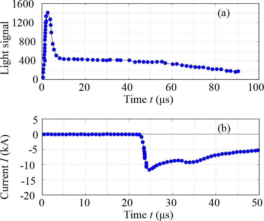
(a) Light signal (Fig. 2 [29]) and (b) current waveform (Fig. 4 [30]) of lightning. The 10/90 rise time of the light signal is approximately 1.15 μs, and that of the current is approximately 1.13 μs. Since a strong correlation between current and light intensity has been shown up to the peak of the lightning current, the current waveform up to the peak can be directly interpreted as the light intensity [29].
We will analyze the light from the light source incident on the image sensor. The radiant energy Qe (J) of light incident on a pixel can be expressed as the integral of the radiant flux Φe (W) with respect to t, as follows:
We assume that the light source emits light with a constant brightness, referred to as DC light. The radiant flux of this light is constant and can be expressed as follows (Fig. 4 (a)):
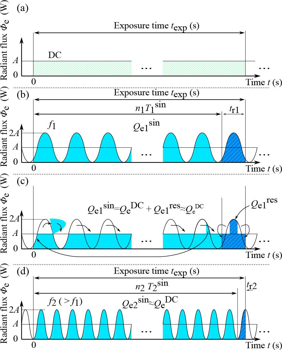
Radiant flux Φe (t) vs. time t. (a) The radiant flux
The radiant energy
We assume that the light source emits rapidly changing sinusoidal light with frequency f1. The radiant flux of the sinusoidal light with frequency f1 is given by (Fig. 4 (b)):
Since the period of the sinusoidal light is given by
Dividing the integral interval of the second term in (9), we obtain:
Since the second term in (10) vanishes, we have (Fig. 4 (c)):
When the exposure time texp is much larger than the period
From Fig. 4 (d), the residual
Equations (13) and (14) indicate that the radiant energy of sinusoidal light is approximately equal to that of constant-brightness light, regardless of the frequency change of the sinusoidal light. If the condition that the exposure time is considerably greater than the period of the sinusoidal light is satisfied, the radiant energy of the sinusoidal light converges to the radiant energy of the light with constant brightness, regardless of the frequency (Fig. 4 (d)). This study is based on this relationship.
In this study, we utilised three cameras and three lenses, as summarized in Table 1 and depicted in Fig. 5. The cameras and lenses were sourced from renowned manufacturers, specifically CamC–Cf18-55, CamN–Nf18-55, and CamP–Pf12-32.
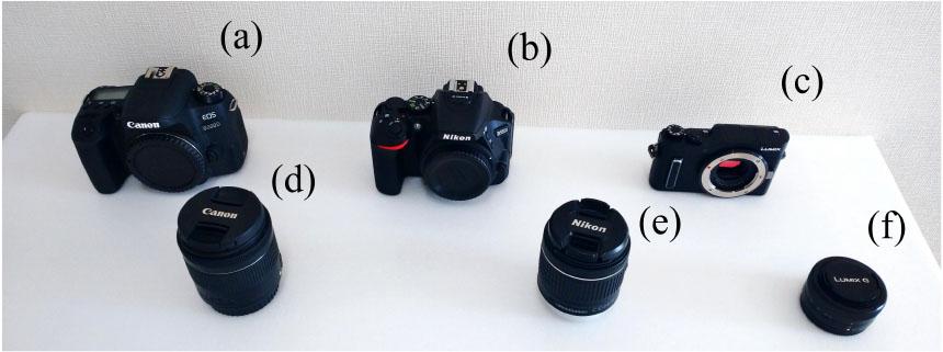
Digital cameras and lenses used: (a) CamC, (b) CamN, (c) CamP, (d) Cf18-55, (e) Nf18-55, and (f) Pf12-32.
Fig. 6 shows the integrating sphere used in this study, along with its reflectance ρ. The open port of the integrating sphere had a circular opening 15 cm in diameter and was mounted on a translucent, milky-white square diffuser measuring 17×17 cm2. Within the open port, the area emitting uniform light was a circle with a diameter of 12 cm. The pigment inside the integrating sphere is matte white, and its reflectance ρ is approximately 95 % over the wavelength range λ = 450–780 nm. While the reflectance ρ for purple light (λ < ∼ 450 nm) is significantly lower, this does not affect the study, as the focus is on analyzing the high-speed photoresponse of the image sensor.
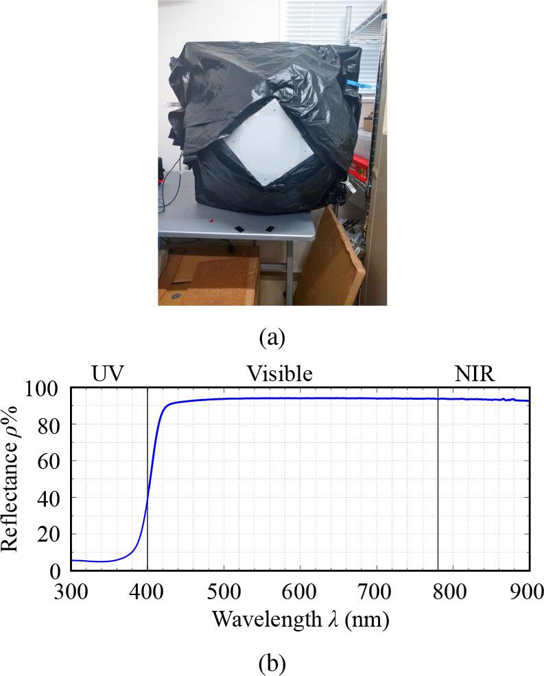
(a) Front view of the integrating sphere used in the study, and (b) reflectance ρ of the white pigment coating the interior of the integrating sphere.
We developed an LED light source (Fig. 7) capable of emitting sinusoidal light in the frequency range from DC to 1 MHz, along with a photosensor (Fig. 8) to analyze the light. The LED light source consists of an LED driver and a light-emitting component comprising three LEDs. The LED driver incorporates a constant-voltage circuit, a summing amplifier, a voltage divider, and a transconductance amplifier, all housed in a shielded box. The LED driver is connected to an external oscillator and a DC-stabilized power source. The frequency of the LED driver is controlled within the range from DC to 1 MHz using the external oscillator. The light-emitting component is connected to the LED driver via two 1.5 m BNC coaxial cables and is positioned inside the integrating sphere. To monitor the LED current, light from a red LED inside the LED driver is directed outside via an optical fiber, where it is detected by the photosensor (Fig. 8). The primary electronic components of both the LED driver and the photosensor are described in the Appendix.
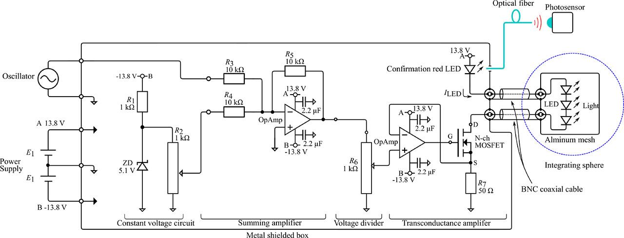
Schematic circuit diagram of the sinusoidal light source. To minimize noise, the LED driver is housed in a metal aluminum shielded box, while the light-emitting component is placed inside an aluminum mesh box. The sinusoidal wave (peak voltage Vp = 0.5 V, peak-to-peak voltage Vpp = 1 V) from the oscillator and the bias voltage (Vbias = 0.5 V) from the constant voltage circuit are input to the summing amplifier.
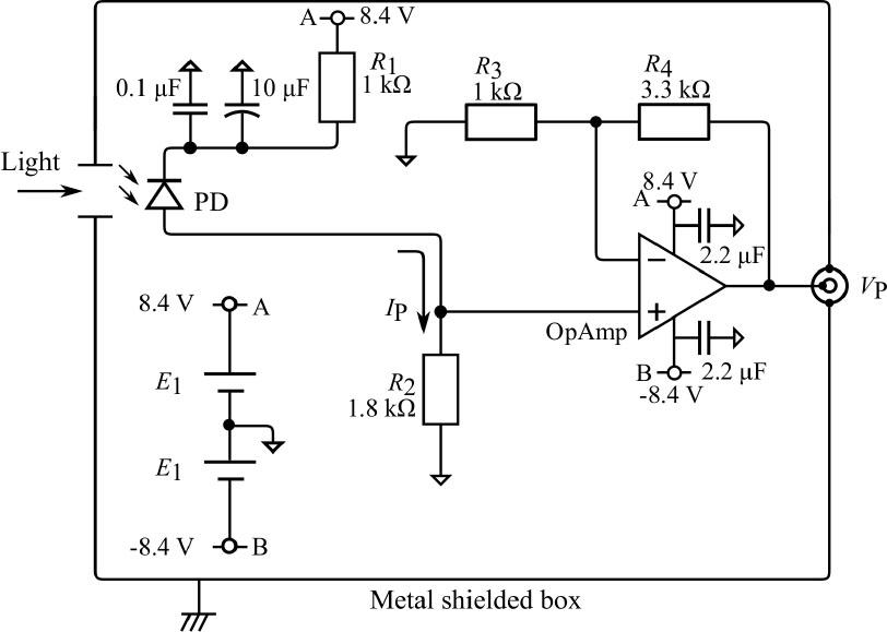
Schematic circuit diagram of the photosensor. Due to the small photocurrent IP (in the range of several tens of microamperes), the output voltage VP is amplified by a factor of 3.3 using the non-inverting amplifier, with the voltage across the shunt resistor R2 serving as the input.
Photography was conducted to analyze the high-speed photoresponses of the three camera image sensors, as shown in Fig. 10. The lens tip of each camera was positioned in contact with the diffuser of the integrating sphere. Table 2 outlines the camera settings used for the photography.
Camera settings for photography. Brightness information is influenced by the exposure time t, ISO gain, focal length f, and F-number F/#. The exposure time and ISO gain are directly related to the image sensors, while the focal length and F-number pertain to the lenses used.
| Combination | Camera | Lens | ||
|---|---|---|---|---|
| Camera-Lens | t (s) | ISO | f (mm) | F/# |
| CamC-Cf18-55 | 1 | 100 | 18 | 4 |
| CamN-NCf18-55 | 1 | 100 | 18 | 4 |
| CamP-Pf12-32 | 1/2 | 200 | 13 | 4 |
The light frames for all three digital cameras were captured in a single instance, and these frames were analyzed in the Bayer data format. We examined four pixels from the blue (B) channel, eight from the green (G) channel, and four from the red (R) channel, all located within the central 4×4-pixel section (Fig. 9) of the RAW image data in the Bayer format. Prior verification confirmed that no hot or cool pixels were present within the central 4×4-pixel area. The RAW data for these cameras are 14-bit for CamC and CamN, and 12-bit for CamP; however, these were converted to 16-bit for analysis. The pixel values from each camera were averaged for each B, G, and R channel, as shown in (15),
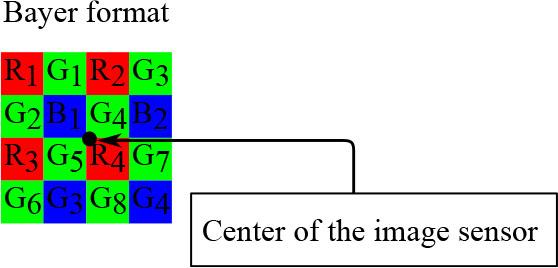
Central 4 × 4 pixels of the RAW data in Bayer format. This region includes 4 pixels for the blue (B) channel, 8 pixels for the green (G) channel, and 4 pixels for the red (R) channel.
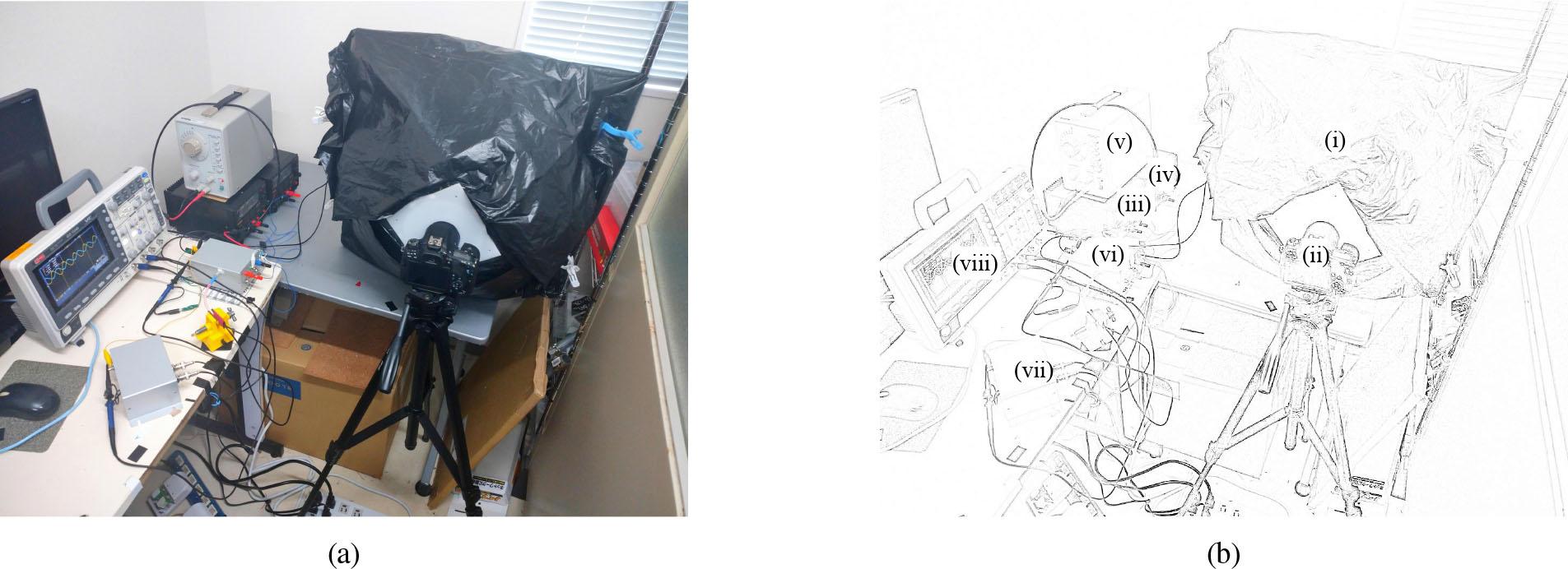
(a) Setup of the camera and integrating sphere, and (b) arrangement of each measurement module. The positioning of each module is as follows: (i) integrating sphere, (ii) digital camera, (iii) and (iv) DC-stabilized power supply, (v) oscillator, (vi) LED driver, (vii) photosensor, and (viii) oscilloscope. To shield ambient light, the integrating sphere and camera were covered with a black plastic sheet during photography.
Dark frames for the B, G, and R channels of the three cameras were captured by attaching a light-shielding cap to the end of the lens. Prior to the main optical measurement experiment, preliminary dark-frame capture experiments were conducted. We captured 290 dark frames with CamC, 380 with CamN, and 150 with CamP. For exposure times of 1 second or less, a sample of 10 dark frames from each camera was found to be sufficient for achieving the required precision. The dark frames were captured 290 times for CamC, 380 times for CamN, and 10 times for CamP, following the settings in Table 2. These frames were then averaged. The pixel values from the central 4 pixels of the averaged dark frames for the B, G, and R channels were used as the dark values.
The absolute and relative errors of the pixel values were calculated for data analysis. The absolute error was determined as Eabs = VDC − V, and the relative error was given by Erel = (VDC − V)/VDC, where V represents the pixel value at each frequency, and VDC corresponds to the pixel value under constant brightness light. In these error equations, VDC was considered the true value.
The dark values used for dark calibration are summarized in Table 3. From this point onward, we define the pixel values of the image sensors as those calibrated with the dark values listed in Table 3.
Dark values of the image sensors in three cameras.
| Camera | B | G | R |
|---|---|---|---|
| CamC | 2045.90 | 2045.28 | 2045.72 |
| CamN | 2408.16 | 2406.07 | 2408.68 |
| CamP | 2288.0 | 2282.0 | 2284.0 |
The current flowing through the LED of the sinusoidal light source can be monitored by measuring the voltage across the shunt resistor R7 (Fig. 7). Light from the confirmation red LED (Fig. 7) inside the LED driver is guided outside through an optical fiber and subsequently measured by the photosensor (Fig. 8). Fig. 11 displays the output waveforms of the sinusoidal light source and photosensor when driven at frequencies of 10 Hz and 1 MHz. As frequency increases, the operational amplifier gain decreases, and phase shift occurs, but both the sinusoidal light source and the photosensor function correctly up to 1 MHz.
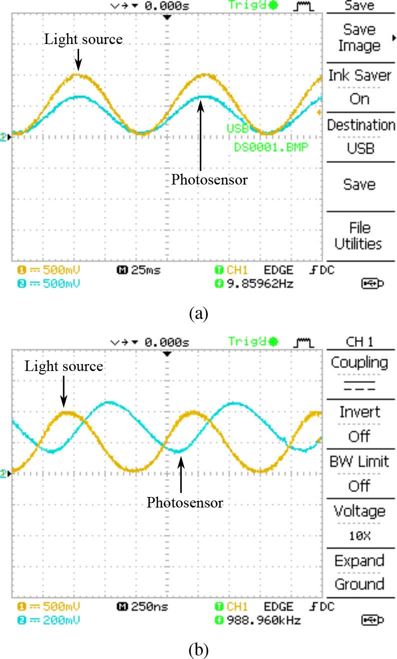
Output waveforms of the sinusoidal light source and photosensor at frequencies of (a) 10 Hz and (b) 1 MHz.
The photoresponses of the three camera image sensors were measured, as shown in Fig. 12. In this figure, the pixel values V for CamC, CamN, and CamP remained nearly constant across the frequency range from DC to 1 MHz. Notably, CamN showed greater variation in pixel values than CamC and CamP. This variation is more clearly observed through the absolute error Eabs and relative error Erel in Fig. 12.
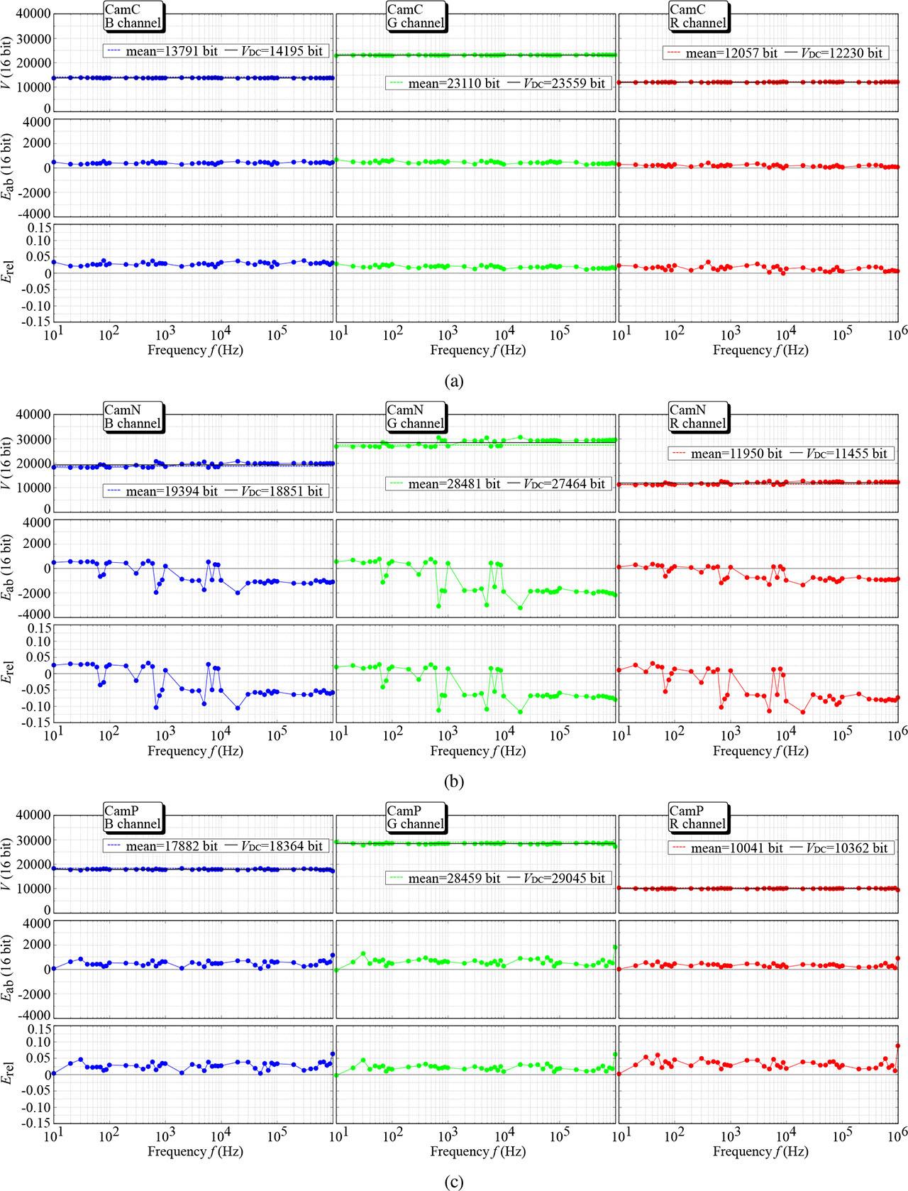
Pixel value V versus frequency f, absolute error Eabs versus frequency f, and relative error Erel versus frequency f for (a) CamC, (b) CamN, and (c) CamP. The results for the B, G, and R channels are presented from left to right. The solid and dashed horizontal lines represent the DC pixel value VDC and the mean pixel value, respectively.
A common trend observed across all three cameras (CamC, CamN, and CamP) in Fig. 12 was a significant difference in the average pixel values V between the B, G, and R channels. This discrepancy is attributed to the transmittance of the on-chip color filter and the quantum efficiency of the image sensor, rather than the photoresponse of the sensor. Therefore, the difference in average pixel values between the B, G, and R channels can be disregarded. The minimum absolute error for the B, G, and R channels was nearly identical across all three cameras. However, CamC demonstrated the smallest average and maximum absolute errors, followed by CamP and CamN. The relative error Erel results in Fig. 12 indicate that the average relative error for CamC and CamP was approximately 3 % or less, while for CamN it was approximately 5 %. This discrepancy is likely due to slight compression of the RAW data for CamN.
As previously mentioned, the pixel values of the image sensor remained almost constant up to 1 MHz, with only slight errors. These results suggest that the image sensor accurately captures sinusoidal light within the frequency range from DC to 1 MHz. In other words, if the frequency of the sinusoidal light is below 1 MHz, all the conditions (1)–(5) outlined in subsection 2 - A were correctly met. This study focused specifically on condition (1), and our experimental results support the prediction that each photodiode in the image sensor successfully generated electrons through the photoelectric effect. A potential concern was that the carrier concentration could temporarily increase rapidly due to the 1 MHz sinusoidal light, potentially leading to a decrease in carrier lifetime. However, in practice, even at 1 MHz, we obtained results that align with theoretical expectations. Furthermore, these results validate the theoretical analysis method we developed.
Assuming a lightning rise time of 0.5 μs, the abrupt brightness change can be approximated by sinusoidal light with a frequency of 1 MHz and a period of 1 μs. For a rise time of 1 μs, the brightness change can be approximated by sinusoidal light with a frequency of 500 kHz and a period of 2 μs. Fig. 12 demonstrates that the image sensor correctly captured sinusoidal light up to 1 MHz. Similarly, the rapid brightness fluctuations during the rise time of most lightning events were also accurately captured. These results further suggest that the camera is capable of capturing objects and phenomena with rapid brightness changes, such as spark discharges in electrical engineering, aurora borealis in solar-terrestrial physics, and transient astronomical events in time-domain astronomy.
It is important to note that our findings do not define the upper limit of photoresponse for the three image sensors at 1 MHz. The photoresponse characteristics of the image sensor photodiodes, including rise/fall times and cutoff frequencies, depend on the physical properties of the semiconductor material and the design parameters. In particular, enhancement of the cutoff frequency can be achieved through various approaches, including extension of the photodiode depletion region, control of defect and impurity concentrations serving as carrier recombination centers, increase of the FD region capacitance CFD, and realization of a high-sensitivity SFA. Nevertheless, none of these approaches alone leads to a decisive improvement, and optimization must be achieved through balancing the trade-offs among sensitivity, response speed, noise performance, and saturation characteristics. From the viewpoint of digital camera end users, when photographing subjects with rapidly changing brightness, the photoresponse of the image sensor should be verified using the time-integration analysis method outlined in this study.
The limit of the time-integration analysis method developed in this study is determined by the lower of the maximum frequencies of both the light source and the photosensor. For example, the maximum frequency of the sinusoidal LED light source used in the experiment was approximately 1 MHz, while the maximum frequency of the photosensor is approximately 2 MHz. The limit of the experiment with the developed light source and photosensor was up to 1 MHz. We are fortunate to have demonstrated that image sensors can capture lightning, one of the fastest natural phenomena.
For future work, developing a light source for high-speed analysis requires frequencies above 1 MHz. While silicon-based visible LEDs and infrared LEDs or laser diodes for high-speed communication are options, we will choose visible light laser diodes. This is because it provides the necessary high frequency while remaining within the visible spectrum, which is required to analyze the characteristics of image sensors.
Similarly, developing a photosensor for high-speed analysis presents its own challenges. While silicon-based photosensors have fast response times (typically on the order of nanoseconds), internal electronic components limit their actual speed to tens or hundreds of MHz. Furthermore, the complex circuit design for both the photosensor and the laser diode light source will be a challenge, as most high-speed components are surface-mount devices.
The upper limit of the cutoff frequency for image sensors used in ordinary cameras is probably between 1 MHz and 100 MHz at most. This limit depends not only on the semiconductor’s carrier concentration and mobility, but also on the pixel’s internal nanoscale structure. Without detailed information, which is not provided in manuals or data sheets, it is not possible to predict the cutoff frequency through theoretical or numerical calculations. Therefore, to analyze rapid luminous phenomena using image sensors, it is necessary to experimentally determine whether the image sensor can accurately capture light at the same frequency as the rapid brightness changes. In this study, we developed this experimental method.
To investigate the photoresponse of the image sensors in three digital cameras, we developed an LED light source capable of emitting sinusoidal waves over the frequency range from DC to 1 MHz, along with a photosensor to measure these frequencies. Using this LED light source, we generated sinusoidal waves and irradiated the image sensors with them. Our study reveals that digital cameras can accurately capture sinusoidal waves up to frequencies of 1 MHz. While image sensors may be capable of capturing sinusoidal waves at frequencies above 1 MHz, we could not determine the exact cutoff frequency or the limit of the photoresponse of the image sensor. Since a 1 MHz sinusoidal wave approximates the lightning waveform during its rise time, (approximately 0.5 to 1 μs), the image sensors in the three cameras tested accurately captured the rapidly changing light of lightning.
The findings of this study do not suggest that all commercially available image sensors are capable of accurately capturing rapidly changing light that can be approximated by a 1 MHz sinusoidal wave. Rather, from a measurement perspective, when encountering rapidly changing brightness, end users must assess the photoresponse characteristics of the image sensor using the time-integration analysis method presented here. There are currently several special-purpose nanosecond-order cameras with extremely limited applications, and multiple manufacturers are continuing to develop high-speed optical cameras with nanosecond-order response. Even when using such a camera with nanosecond-order photoresponse to capture images of rapid brightness changes, it is still possible for the user to assess the performance of the image sensor using the time-integration analysis method. These results will contribute not only to lightning research but also to various other fields (e.g., natural sciences, applied sciences) based on photometry using digital cameras.
We believe it is essential to explore the potential of digital cameras to capture rapid light changes beyond 1 MHz. In the future, we plan to develop a light source that emits sinusoidal light at frequencies ranging from 1 MHz to several hundred MHz, as well as a photosensor capable of detecting this light, to investigate the limits of image sensors.
This study investigated the optical characteristics of commercially available digital cameras. There is no specific rationale for selecting the three cameras used in this study, and the results do not suggest any superiority or inferiority among manufacturers or products.