
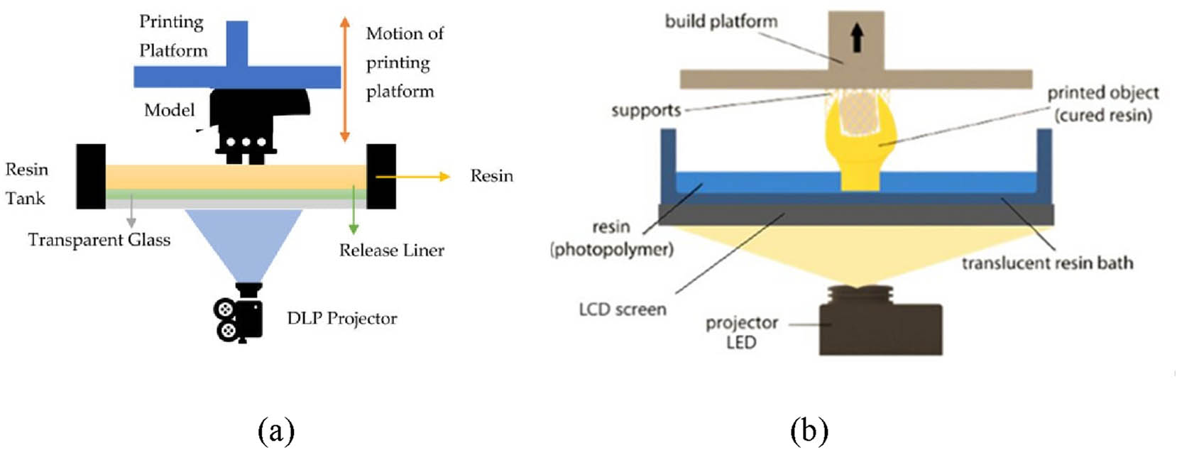
Figure 1
(a) Schematic representation of the DLP method (upstream) [3] and (b) schematic representation of the LCD method [4].
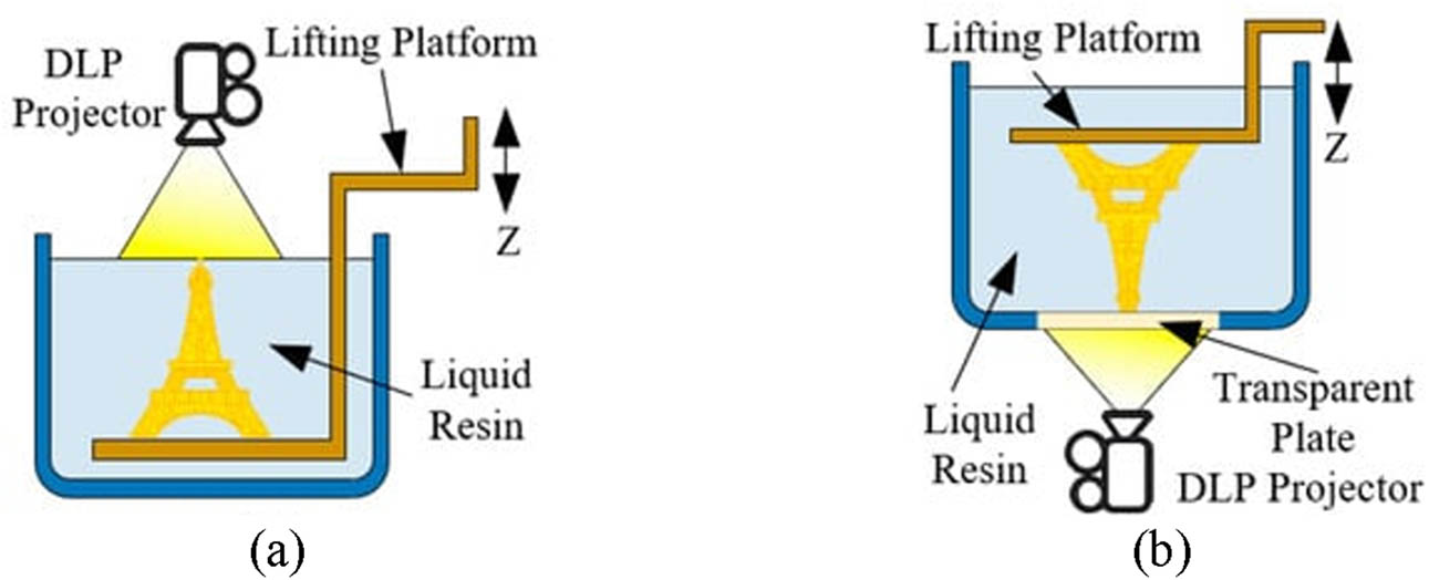
Figure 2
(a) Downward DLP projection and (b) upward DLP projection [13].
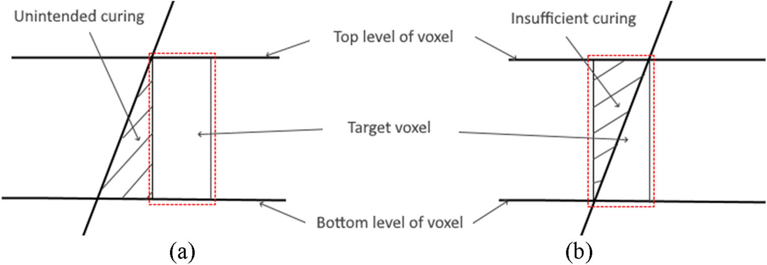
Figure 3
Schematic illustration of voxel curing defects induced by oblique light incidence: (a) Unintended curing of material adjacent to the target voxel and (b) insufficient curing within the target voxel caused by reduced effective exposure.
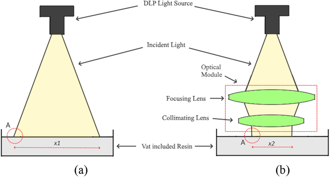
Figure 4
DLP 3D printer schematics: (a) Without optical module and (b) with optical module.
Table 1
Printing parameters with and without optical module
| Parameters | Printing parameters without optical module | Printing parameters with optical module |
|---|---|---|
| Layer thickness | 0.065 mm | 0.065 mm |
| Number of layers | 82 | 82 |
| Lift and sequence time | 5,000 ms | 5,000 ms |
| Exposure time | 2,500 ms | 100 ms |
| First layer exposure time | 10,000 ms | 4,000 ms |
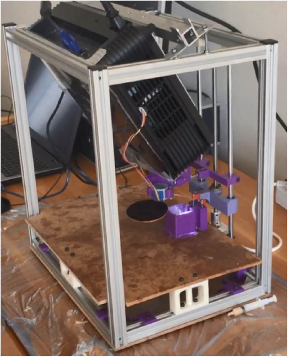
Figure 5
General view of the experiment setup.
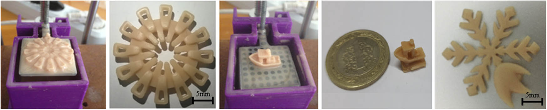
Figure 6
Some printed samples for visual and microscopic investigations.
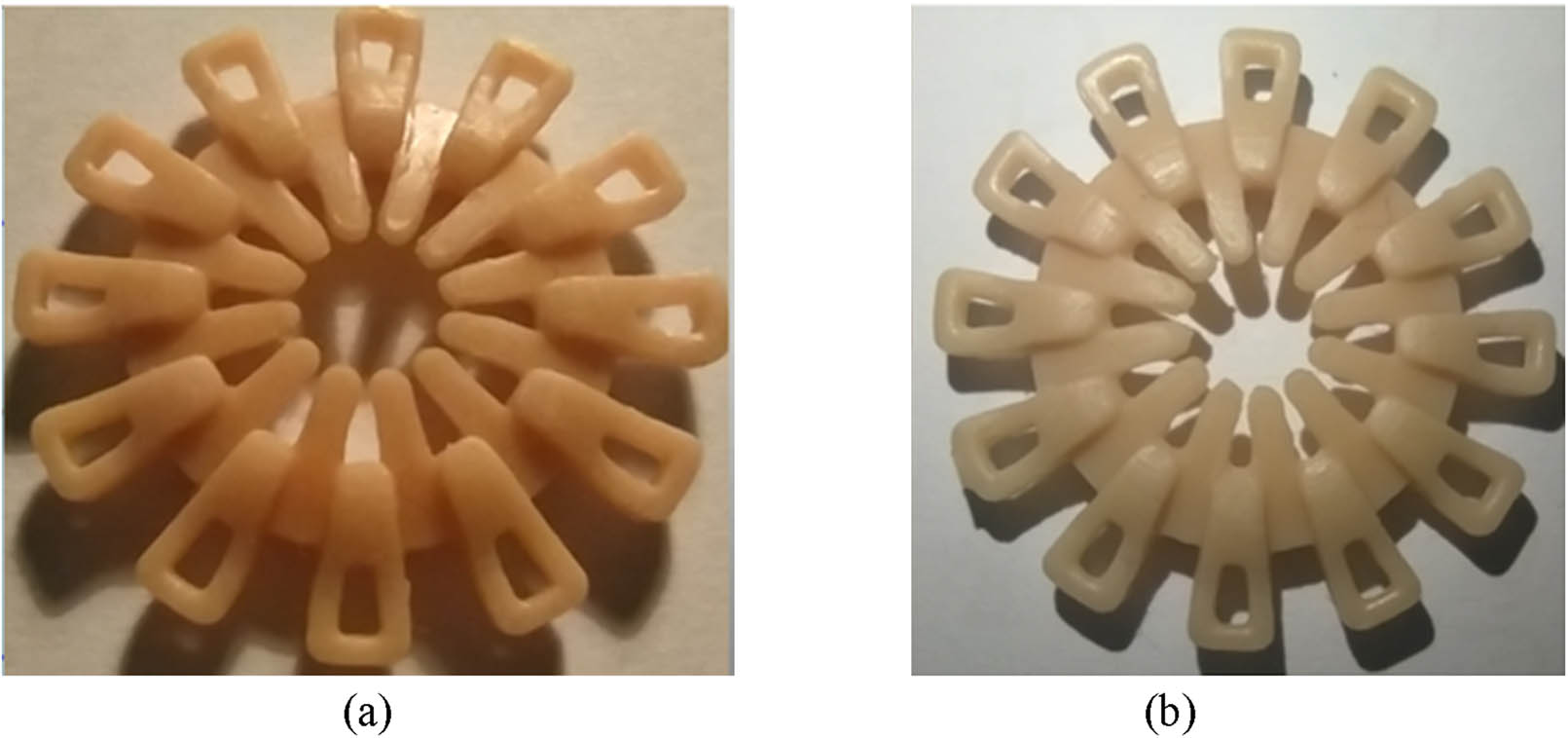
Figure 7
(a) Part printed without optical module and (b) part printed with optical module.
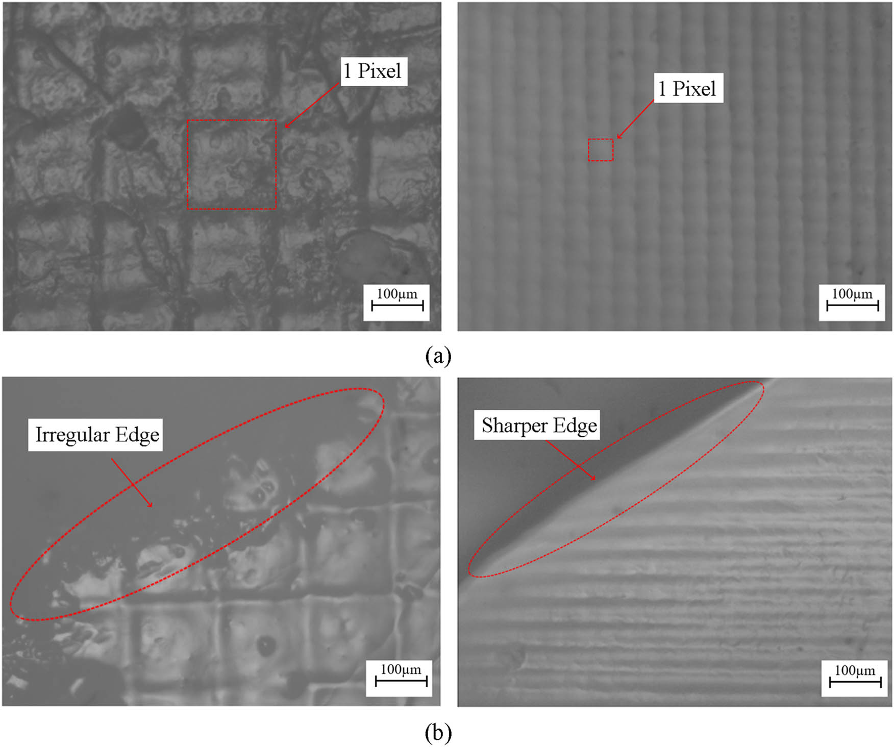
Figure 8
(a) Images from the middle parts of the parts (without optical module on left and with optical module on right) and (b) images from the angled edges of the parts (without optical module on left and with optical module on right).
Table 2
Impact of optical system on resolution and printing performance
| Parameters | Without optical module | With optical module | Improvement |
|---|---|---|---|
| Layer exposure time | 2,500 ms | 100 ms | 25× reduction |
| Total printing time | 00:10:45 | 00:07:17 | 1.45× faster |
| Pixel size | 168.1 µm ± 3.4 | 44.5 µm ± 2 | ∼3.8× reduction |
| Edge definition/pixel array | Irregular/blurred | Homogeneous/sharp | Visual enhancement |