The search for chemical synthesis methods to prepare nanocrystals of organic and inorganic compounds with experimental physical and chemical parameters controllable in the laboratory has motivated the search for optimal parameters in crystal growth, which can achieve high surface areas through the rational design of nanocrystals ranging from aggregation, chemical composition, crystallinity phase, size, morphological surface [1], and shape control or at least the protocols have proven to be reproducible and controllable [2]. The control of the surface and structural morphology of a nanocrystal and its correlation with the optical response in a certain region of the electromagnetic spectrum allows adequate control of its properties and improvement of its usefulness for a specific application. The example of multiple applications in the photocatalytic efficiency also largely depends upon the nanocrystals’ morphology, grain size, and specific surface area [3]. In particular, cadmium carbonate (CdCO3) is an inorganic nanomaterial that presents different morphologies with interesting surface geometries, nanowires, nanoribbons, nanorings, sphere-like architectures [4], and square/cube facets [5]. Cadmium oxide (CdO) is a nanomaterial with outstanding structural and optical properties in the absorption of the visible region of the electromagnetic spectrum [6]. These properties make them applicable in several fields such as photonics [7], electronics, biosensors, and treatment of environmental hazards [8]. Various research groups have reported experimental preparation techniques and potential applications of CdO nanocrystals [9]. However, the simplest and easiest method to systematically examine the preparation of CdO is via the thermal decomposition of CdCO3 [10]. Chemical bath deposition (CBD) offers outstanding capabilities, such as scalability [11], self-limiting growth [12], low cost [13], and simple equipment [14]. To the best of our knowledge, there are only a few publications on CdCO3 [15] and its application in the photodegradation of methylene blue. Although there is no vast information related to the photocatalytic activity reported by CBD, which is a cost-effective technique [16] because the equipment required is inexpensive, making it attractive for producing thin films easily scalable for industrial applications, [17] its versatility due to the possibility of depositing a wide range of materials, including oxides, sulfides, and chalcogenides, make it applicable in various fields such as solar cells, sensors, and coatings [18].
In this study, the experimental results showed that CdO nanoparticles prepared from CdCO3 followed an autocatalytic reaction [19]. In this study, we analyzed the optical and structural properties of the CdCO3 to CdO transition by thermal annealing, obtained using the green chemistry technique CBD [20]. Additionally, the rate of photocatalytic degradation of methylene blue was determined [21].
The aqueous solutions containing the progenitor reagents used here are prepared at room temperature using deionized water mixed in the following order: Cd(NO3)2, KOH, NH4NO3, and CS(NH2)2. The mixture is stirred uniformly, at a constant temperature of ∼20°C for 40.0 h. The steps are shown in Figure 1.
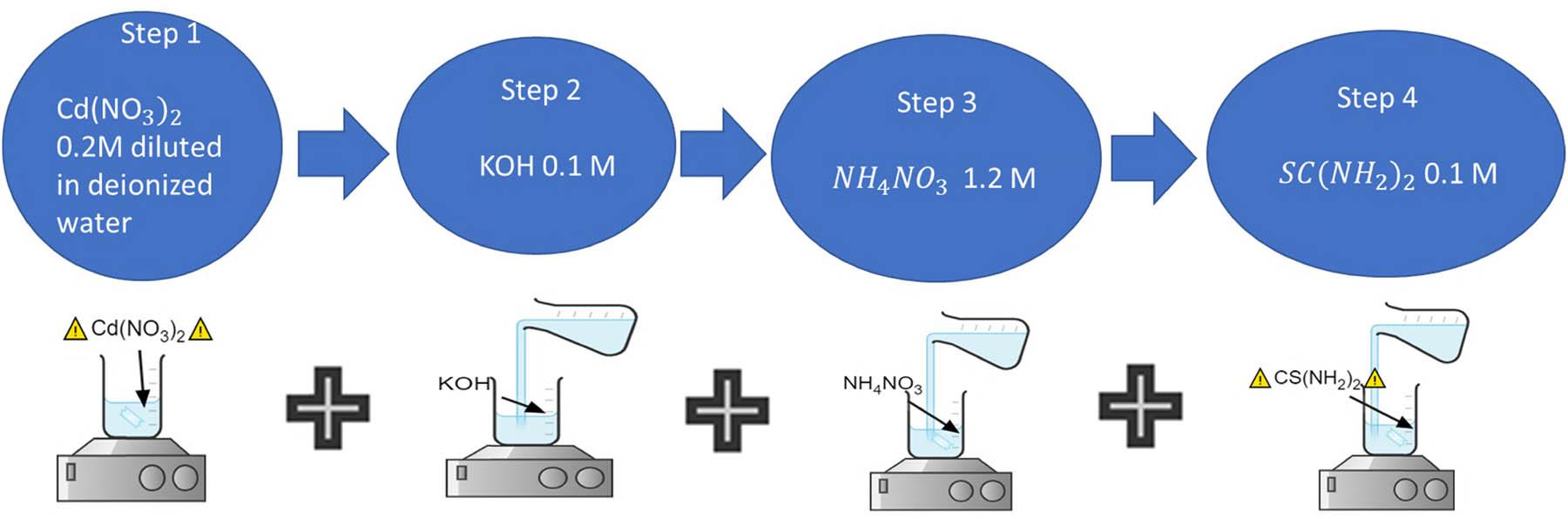
Schematic of the chemical deposition of CdCO3 powder.
Next, we present the equilibria associated with the chemical kinetics of crystal growth for the systematic preparation of CdCO3 nanocrystals.
The aqueous solution containing the Cd+2 cation captures OH− ions present in the alkaline medium (pH ∼8.3) under optimal conditions proposed by us, generating the suspension of milky appearance of cadmium hydroxide Cd(OH)2(aq):
A noticeable phenomenon is observed when the nanocolloidal suspension of Cd(OH)2(as) turns into a clear solution by the direct addition of an aqueous solution of NH4NO3, indirectly generating the tetramine cadmium coordination complex [Cd(NH3)4]2+ cation [22]. This stage is considered to determine the cation used to obtain the oxide, hydroxide [23], or a mixture of both inorganic compounds associated with the final product obtained [24]. In other words, the properties of the coordination complex cation are associated with the physicochemical characteristics [25] of the cation used (Cu2+, Co2+, Zn2+, Nd3+, Sm3+, etc.) in crystal growth [26].
Therefore, the physicochemical parameters associated with this stage are the subject of various publications:
The [Cd(NH3)4]2+ cation slowly dissociates and captures the
Figure 2 shows a typical molecular diagram of the carbonate ion related to the delocalization of π-electrons. The relative thermodynamic stability of the molecular configuration of the
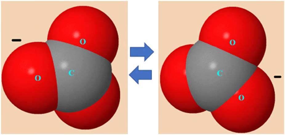
Molecular diagram of the carbonate ion related to the delocalization of π-electrons.
The carbonate ion (
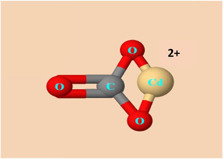
Molecular diagram of CdCO3.
The following equipment was used for the characterizations. Scanning electron microscopy (SEM) with the technique using Voyager II quantitative X-ray microanalysis in an SEM 1100/1110 system from Noran Instruments was used to observe the morphology. FTIR spectra were recorded using a Perkin Elmer spectrophotometer in the wavelength range of ∼500–4,000 cm−1. X-ray diffraction (XRD) patterns were recorded on a Siemens D500 diffractometer, using the Cu Kα line to obtain the corresponding crystal structure.
Figure 4 shows the micrographs obtained by the SEM technique of polycrystalline thin solid films at (a) 30°C, (b) 150°C, (c) 300°C, (d) 400°C, and (e) 500°C. According to the morphological images of the thin solid films, plates assembled with a flat and smooth surface can be observed, supported on the surface of a small nanocrystalline thin layer. Granular stacks feature individual crystalline entities with pyramid-like geometries stacked in different directions in a disorderly fashion. The average length of the crystals was ∼2–5 μm. Another interesting surface characteristic of the thin solid films is the crystalline grain boundaries, which are very close to each other. Usually, the morphological and structural properties present a wide correlation with the optical properties, which are of wide interest in various scientific and technological applications [28]. It is possible to observe directly in SEM images that the effect of the TAT does not significantly modify the crystalline morphology of the thin solid films; this is best reflected in the histograms in Figure 3 for all samples (a), (b), and (c), where the average nanoparticle size does not vary significantly (2–5 μm). Generally, drastic morphological changes related to the effect of TAT have been reported in morphological studies of inorganic nanocrystals using SEM [29]. The experimental techniques applied for chemical synthesis in the preparation of inorganic compounds have been exhaustively investigated and associated with the phenomenon of crystalline growth, considering the geometric properties of the crystal and meticulously controlling the optimal physical and chemical parameters involved [30]. Such variations often correspond to a drastic change in the structural and physicochemical properties and offer an opportunity for nanocrystal fine-tuning [31]. Various theoretical-experimental models have been proposed to study the evolution of crystalline growth, considering the origin of morphology as a complex phenomenon that is difficult to fully understand [32]. Generally, in the phenomenon associated with crystalline growth, the following critical stages have been proposed: (a) creation of nanocolloids and the spontaneous or gradual transformation into long compact crystals and growth of the crystal geometry that acquires greater relative energetic thermodynamic stability, involving various possible precursor phases (amorphous or crystalline), which is governed by the parameters of the environment (chemical or physical); temperature, pressure, concentration of precursor reagents, pH, etc. [33]; and (b) nanonuclei generated by the gradual creation of an active center of minimum relative energy under experimental conditions evolve favorably until reaching the minimum relative energy stability of the crystal, as well as the optimum size.
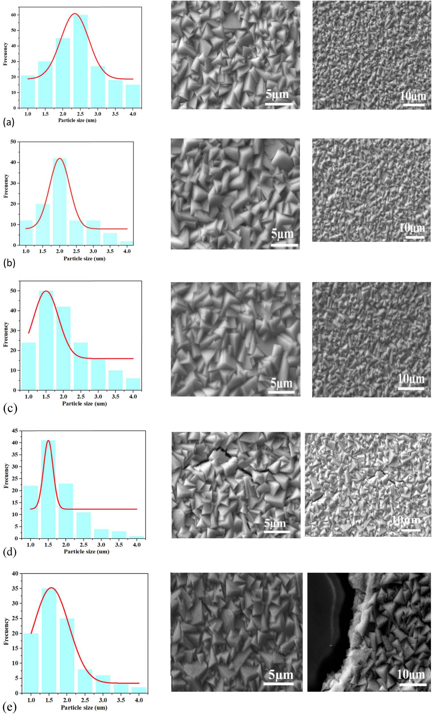
Micrographs and histograms obtained by SEM of the polycrystalline thin solid films at (a) 30°C, (b) 150°C, (c) 300°C, (d) 400°C, and (e) 500°C.
Figure 5 shows FTIR spectra of 30°C, 150°C, 300°C, 400°C, and 500°C thin solid films. The vibration bands in the FTIR spectra, located in the range ∼3,600–400 cm−1, correspond to the characteristic vibrations of the carbonate (
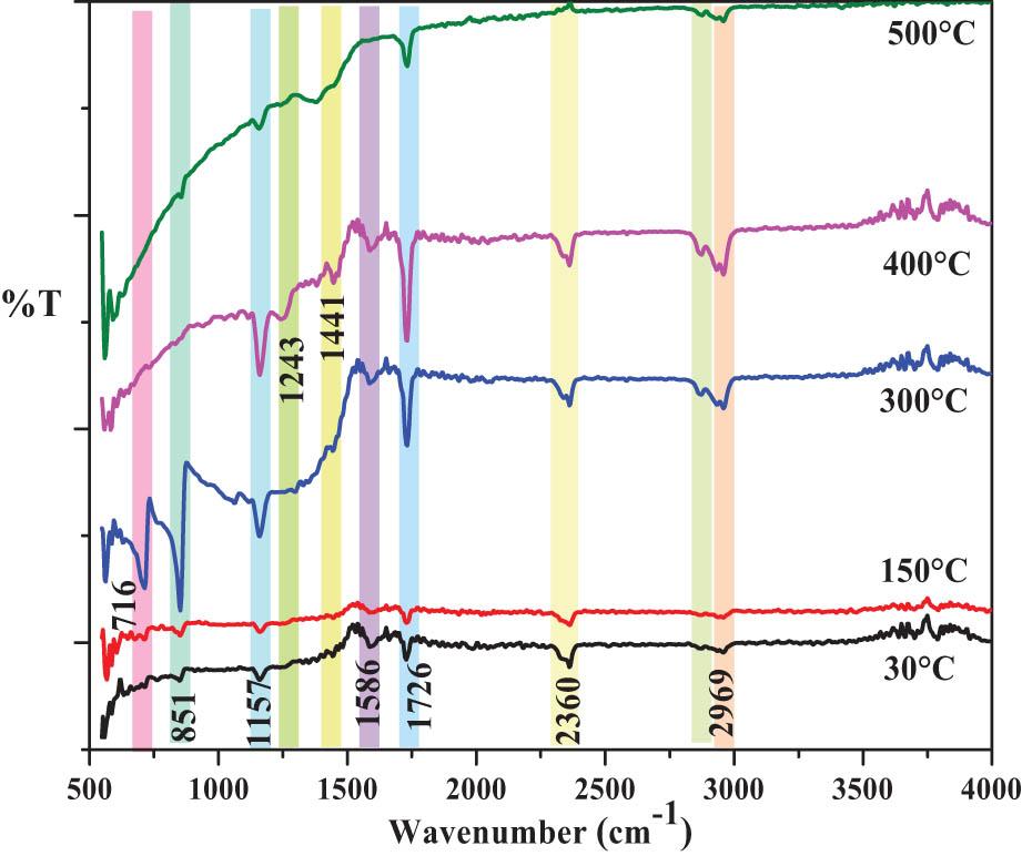
FTIR spectra of the 30°C, 150°C, 300°C, 400°C, and 500°C thin solid films.
The powder of CdCO3 annealed at 500°C decomposes and, at this temperature,
To investigate the structural and microstructural properties of the polycrystalline thin films, the XRD technique is applied. We performed angular scanning (2θ) in the range of 2θ ∼20°–80° on all samples. The XRD diffractograms are arranged in descending order, starting with the 30°C thin solid film, followed by the treated samples (TAT). Figure 6 shows the XRD diffractograms of the thin films, labeled 30°C, 150°C, 300°C, 400°C, and 500°C, respectively. The 30°C, 150°C, and 300°C thin solid films present six angular reflections of different relative intensities when compared with each other. The crystalline reflections recorded at the angular positions located at 2θ ∼23.4°, 30.16°, 32.96°, 36.26°, 48.0°, and 49.66°, associated with the corresponding (012), (014), (116), ( 110), (024), and (116) crystalline planes, were identified with CdCO3 rhombohedral phase, space group Rc-187, according to reported standards (00-042-13-42). In the angular reflections, the presence of materials other than CdCO3 was not recorded, showing that with the CBD technique, it is possible to prepare inorganic materials with acceptable purity. In the 400°C sample, six additional angular reflections emerge at 2θ ∼33.06°, 38.3°, 55.3°, 65.98°, and 69.36°, corresponding to the (111), (200), (220), (311), and (222) crystal planes, respectively, as well as ae decrease in the relative intensity identified in the CdCO3 thin solid films. In the 500°C sample, the crystalline planes associated with CdCO3 completely disappeared, making it possible to identify the crystalline planes of CdO, according to the standards (card number 96-9006674). No other material other than CdO was identified, which implies that the effect of TAT produces the gradual and total transformation of CdCO3 to CdO, obtaining it in pure form. The transition from CdCO3 → CdO is observed in this analysis.
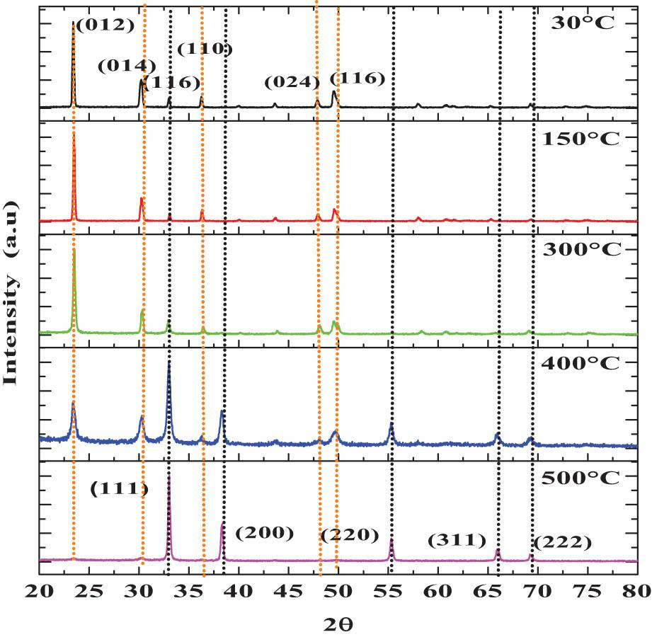
XRD diffractograms of the 30°C, 150°C, 300°C, 400°C, and 500°C thin solid films.
We propose gradual structural evolution according to the following reaction:
The crystalline phase transition of the inorganic nanocrystals examined here implies a complex microstructural phenomenon in the crystalline lattice; these have not yet been specifically presented and must be methodically analyzed. This phenomenon involves spatial disruption around the nucleus of a new phase owing to the inherent volume change. Atomic, molecular, and/or crystalline relaxation during chemical and physical changes produces lattice strain, which in turn affects the nucleation kinetics and dynamics of the transition, as in the case of nanocrystals [37].
The nanocrystals undergo a rhombohedral → cubic phase transition, which is discernible through the loss of rhombohedral features and shifting of high-symmetry reflections. Gradual creation of microstructural changes associated with ion and cation slippage, among other parameters in the crystal lattice; interplanar distance, lattice parameter related to the translation in the corresponding geometric position (lengthening and/or decrease of the lattice parameters) that have the minimum relative crystalline energy, reaching relative thermodynamic stability of the crystal lattice [38]. In this context, it is suggested that the external energy applied serves to rearrange the crystal lattice, thereby selectively creating a new position of minimum crystal energy for each TAT.
The crystal size for each sample was obtained by using the Scherrer equation as follows:
Figure 7 shows the grain size (GS), interplanar distance (ID), and temperature (°C) spectra of the 30°C, 150°C, 300°C, 400°C, and 500°C nanocrystals. The GS decreases from ∼50 to 25 nm in the 30–400°C temperature interval, then presents a drastic increase at ∼43 nm on the 500°C film. The experimental results obtained here provide information on some of the microstructural properties of the nanocrystalline system, which are associated with the gradual transition of the crystalline phase; in this case, it corresponds to CdCO3 to CdO, such as tunable GS, morphology, crystalline phase, tailored porosity, surface area, and stacking faults [39]. On the other hand, the changes at ID present oscillatory behavior, in which it reaches a relative minimum of crystalline energy for a 500°C layer. The microstructural phenomenon is justified in principle by the evolution corresponding to the CdCO3 to CdO transition, which is imperative to consider the disordered crystalline energy change of the nanocrystals in the films subjected to TAT. In turn, the previous arguments focus on the relationship involved in this physical phenomenon associated with spatial distortions of the crystal lattice created by various rearrangements of ions and cations, associated with the different chemical bonds present in the Cd <
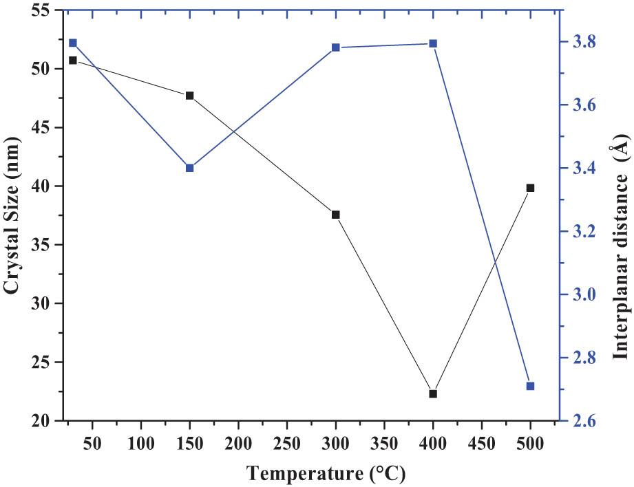
Grain size (GS), interplanar distance (ID), and temperature (°C) spectra of the 30°C, 150°C, 300°C, 400°C, and 500°C nanocrystals.
To calculate the lattice parameters a and c, we apply the following expression:
In Table 1, the lattice parameters a and c, microstrain, and dislocation density (δ) of the 30°C, 150°C, 300°C, 400°C, and 500°C thin films are compiled. The variations of the experimental microstructural parameters registered here have oscillatory behavior, confirming the registered and analyzed results of the GS and ID. The disordered variations are associated in principle with the creation of different chemical bonds in the transition from Cd <
Lattice parameters a and c, microstrain, and dislocation density (δ) of the 30°C, 150°C, 300°C, 400°C, and 500°C thin films.
| Sample (°C) | a (Å) | c (Å) | Microstrain | Dislocation density γ (lines/m2) |
|---|---|---|---|---|
| 30 | 4.947 | 16.263 | 1.144 × 10⁻⁴ | 3.8 × 10¹⁴ |
| 150 | 4.940 | 16.231 | 1.173 × 10⁻⁴ | 4.39 × 10¹⁴ |
| 300 | 4.9231 | 16.292 | 1.19 × 10⁻⁴ | 7.08 × 10¹⁴ |
| 400 | 4.9469 | 16.266 | 3.92 × 10⁻⁴ | 2.01 × 10¹⁴ |
| 500 | 4.9489 | 16.247 | 2.69 × 10⁻⁴ | 6.30 × 10¹⁴ |
The strain of the powders was obtained using the following formula:
The strain values are shown in Figure 8. The observed values are positive, indicating that the strain is tensile. The increment for powder annealed at 300°C and 400°C, and the increment with temperature is due to thermal expansion, and higher strain rates improve the strength. The higher temperature during strain-controlled fatigue tends to reduce the fatigue life for a given strain, and a considerable decrement can be observed at 500°C because of the phase transition from CdCO3 to CdO. In particular, under moderate tensile strains, the materials are suitable for photocatalytic conversion.
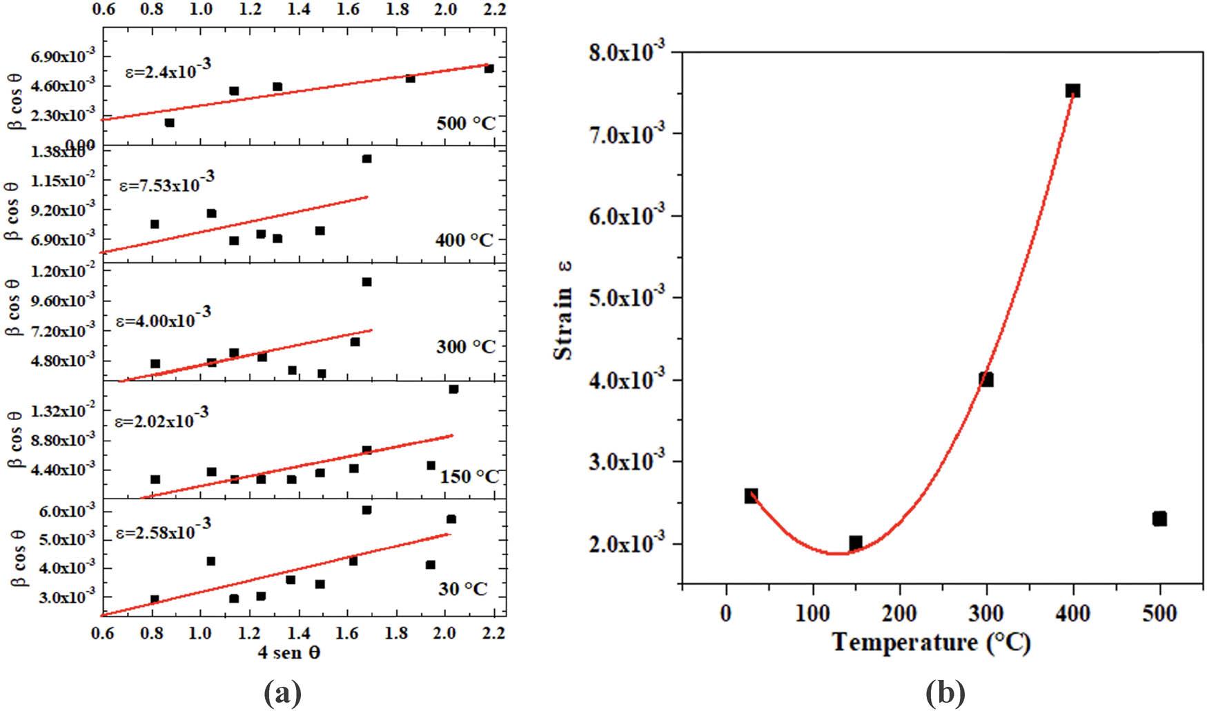
(a) Williamson–Hall plot and (b) strain vs temperature.
The optical properties of transmittance (%T), reflectance (%R), and absorbance (α) of the 30°C, 150°C, 300°C, 400°C, and 500°C thin solid films are examined at the wavelength (λ) located in the UV-Vis region corresponding to λ ∼350–850 nm (∼3.54–1.45 eV) at normal incidence for all the samples. The optical phenomenon commonly recorded in thin films is observed when the incident radiation penetrates the analyzed sample and undergoes a combination of scattering and absorption inside the sample. Therefore, some of the radiation was reflected toward the surface. In the spectral study of %R and %T of various thin films, the standard relationship T + R = 1 is generally applied. Figure 9 displays (a) transmittance (% T), (b) reflectance (%R), and (c) absorbance (α) vs λ (nm) spectra of the 30°C, 150°C, 300°C, 400°C, and 500°C films. The optical phenomenon related to the scattering of incident external radiation in different regions of the electromagnetic spectrum (UV-VI-IR) created by the different changes in morphology, crystalline phase, stoichiometry, grain boundaries, stacking faults, and other properties is correlated with the intrinsic optical properties of each material [42]. Considering the above, related to the different properties of the materials examined in the region used, we have the 30°C and 150°C layers show a similar increase at %T ∼55%. The rough crystalline surface of the 30°C and 150°C thin films presents morphology with various defects, which generate scattering of the incident radiation, which is scattered in different random directions [43]. For the 30°C and 150°C films, the surface roughness is much smoother than that of TAT polycrystalline films. In the Vis-region, %T spectrum, the fundamental electronic valence band (VB) and conduction band (CB), (VB) VB → CB can be seen with a shift located at λ ∼ 450–550 (2.92–2.25 eV). This allows us to visualize in a semi-empirical way the band gap (E g) energy located at the λ (nm) interval examined in our nanocrystals. On the other hand, the 300°C, 400°C, and 500°C films show a drastic increase of %R ∼40–95% at the Vis region. The behavior of α at 30°C and 150°C layers decreases similarly in the region located at ∼350–500 nm (∼3.54–2.48 eV) in both samples, with an insignificant increase for λ > 500 nm. This optical phenomenon is correlated with the different morphological and structural properties and is related to the gradual transformation into a different inorganic material. Similar to surface phenomena, shape-related properties are also apparent, particularly at the nanometer scale. An interesting property, observed in the Vis-region, on the 300°C, 400°C, and 500°C layers, is the existence of an inflection point, which presents a shift in the range of ∼506 nm (∼2.45 eV), ∼536 nm (∼2.31 eV), and ∼556 nm (∼2.23 eV), respectively. From the geometric point of view, the origin of the inflection point in the α spectrum of an inorganic material is considered an optical phenomenon associated with the dispersion of the light beam in single crystals, according to Raleigh dispersion is the predominantly elastic scattering of light or other electromagnetic radiation by particles much smaller than the λ radiation. We propose that this structural behavior is correlated with the scattering of external electromagnetic radiation when λ is greater than the GS [44].
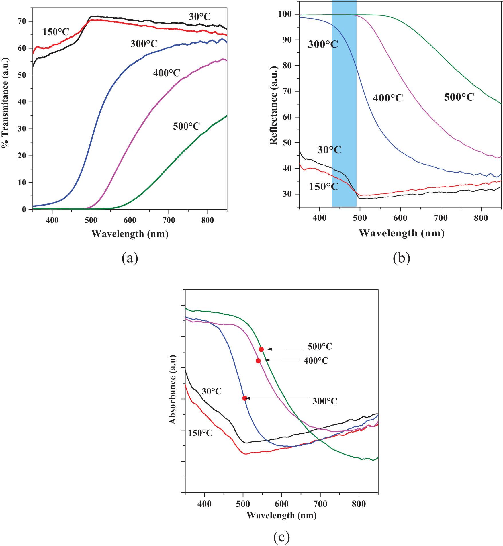
(a) Transmittance % T, (b) reflectance %R, and (c) absorbance (α) vs λ (nm) of the 30°C, 150°C, 300°C, 400°C, and 500°C thin solid films.
Figure 10 shows the normalized absorbance vs wavelength (λ) spectra of the 30°C, 150°C, 300°C, 400°C, and 500°C thin solid films. The 30°C and 150°C samples show an AB of relatively low intensity located at ∼463 nm (∼2.67 eV). However, in the 300°C, 400°C, and 500°C samples, a prominent AB emerges at ∼442 nm (∼2.80 eV), ∼495 nm (∼2.50 eV), and ∼516 nm (∼2.24 eV), respectively. The origin of AB at ∼442 nm (∼2.80 eV) and at ∼516 nm (∼2.24 eV) is associated with the electronic transition, fundamental of CdCO3 and CdO [45]. The oscillatory shift of the relative maximum at AB toward lower energy is correlated with the creation of a CdCO3/CdO solid solution [46] in proportions not quantified here, as well as the variation of the GS of the nanocrystals. The observed AB shift toward higher λ (nm) was ∼74 nm (∼0.16 eV), leading to promoted Vis-region light absorption.
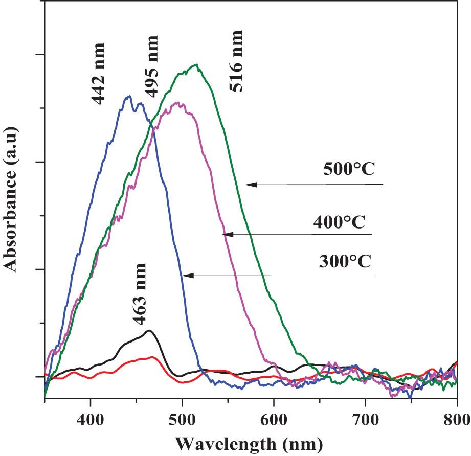
Normalized absorbance vs wavelength (λ) spectrum of the 30°C, 150°C, 300°C, 400°C, and 500°C thin solid films.
For a better understanding, deconvolution was performed and displayed in Figure 11 of the (a) 30°C, (b) 150°C, (c) 300°C, (d) 400°C, and (e) 500°C films. The (a) and (b) films show a weak and broad AB situated in the UV-Vis region at ∼400–500 nm (∼3.10–2.48 eV), recorded at ∼463 nm (∼2.67 eV) and ∼467 nm (∼2.65 eV) for the 30°C and 150°C samples. In the (a) 30°C and (b) 150°C samples, a weak and broad AB is recorded in the UV-Vis region (∼400–500 nm), recorded at ∼463 nm (∼2.67 eV) and ∼467 nm (∼2.65 eV), respectively. The AB was identified in these optical results, and the fundamental transition assigned to the VB → VC of CdCO3 was identified. The small shift toward a higher λ (nm) and lower photon energy (hν) is associated with CdO and, in turn, with the gradual experimental formation of a CdCO3/CdO solid solution promoted by the TAT effect. The deconvolution in (c) and (d) carried out at AB for the 300°C and 400°C films records the AB signals located at ∼392 nm (∼3.16 eV), ∼481 nm (∼2.57), and 661 nm (1.87). Finally, the 500°C film records two AB of different relative intensities located at ∼412 nm (3.00 eV) and ∼516 nm (∼2.40 eV).
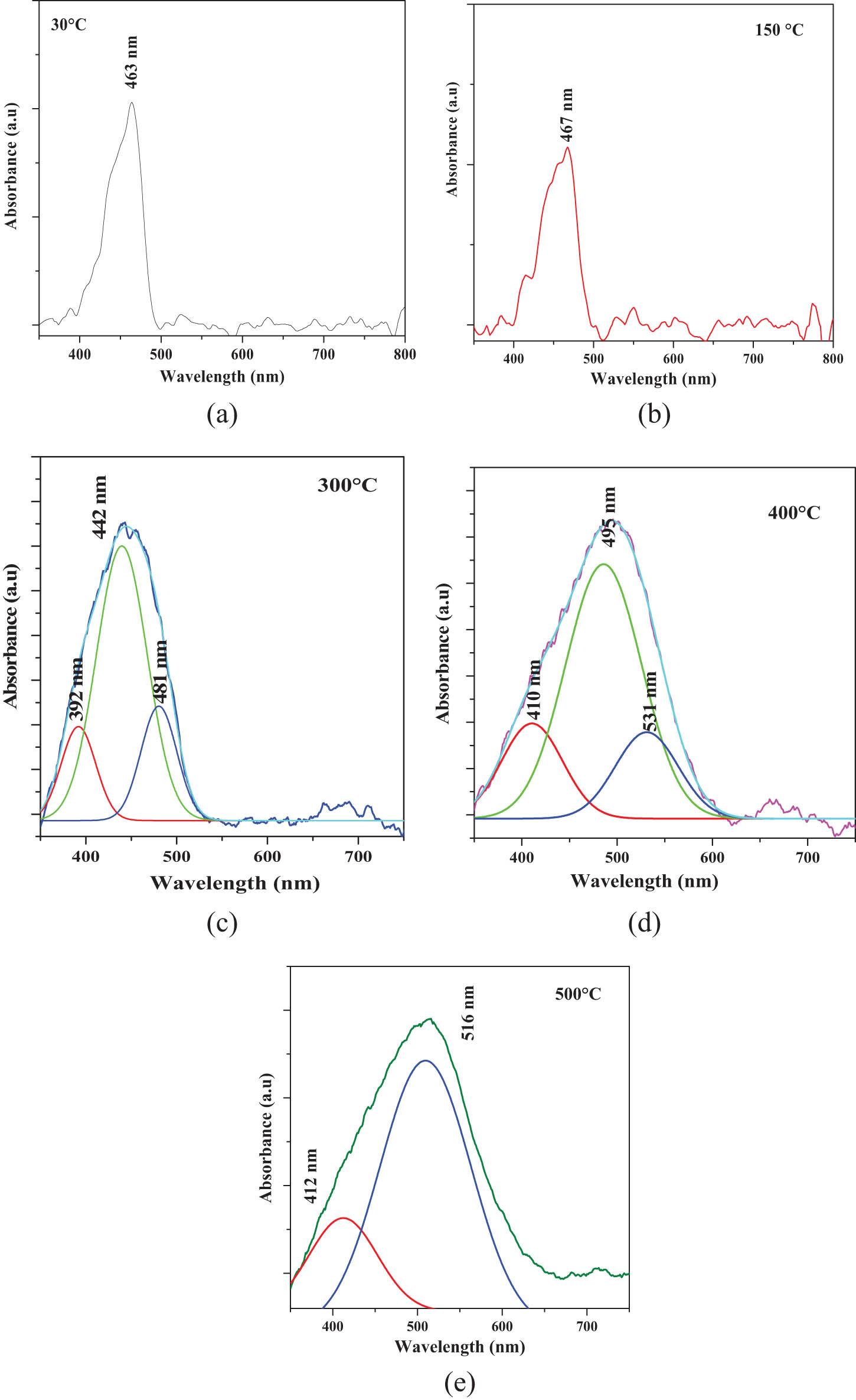
Normalized absorbance deconvolution vs wavelength (λ) spectra of the (a) 30°C, (b) 150°C, (c) 300°C, (d) 400°C, and (e) 500°C films.
Figure 12 shows the spectrum of the derivative of the optical density (OD) to the photon energy d(DO)/dE of the 30°C, 150°C, 300°C, 400°C, and 500°C films. In the d(DO)/dE experimental spectrum, all the films are placed in ascending order, with the 30°C layer in the lower part, followed by 150°C, and so on, to appreciate the differences correlated with electronic transitions related to the VB and the CB at the gradual evolution of CdCO3 to CdO. From this spectroscopic analysis, it is possible to record some AB created by intraelectronic photonic replicas caused by microstructural changes, differences in stoichiometric balance, grain boundaries, and crystalline stacking faults, which are generally recorded by applying this spectroscopic technique. Two broad AB with different relative intensities and higher magnification were recorded at ∼2.58 and ∼2.78 eV. The AB corresponds to the CdCO3 rhombohedral phase assigned to the 30°C and 150°C films, respectively. In the 300°C film, a very broad band with greater relative intensity is located at 2.10 eV. A broad AB situated at ∼1.60 eV and another at ∼1.73 eV are related to the creation of CdO associated with the fundamental electronic transition from CdCO3. The transition to CdO is recorded at the 400°C and 500°C thin solid films. The TAT effect provides the relative and quantitative critical experimental values in the gradual transition, experimentally recorded in the transformation of CdCO3 to CdO.
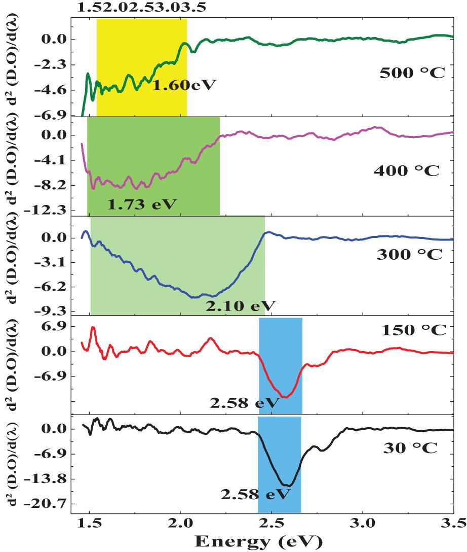
Derivative of the OD concerning the energy of the photon d(DO)/dE spectra of the 30°C, 150°C, 300°C, 400°C, and 500°C samples.
Directly applying the Tauc equation and the previously obtained results of the absorbance (α), we constructed an experimental graph of (αhν)2 vs E (eV). Optical analysis was performed at a photon energy in the range of ∼1.5–3.0 eV, considering the fundamental transitions of CdCO3 and CdO, respectively. The band gap (Eg) energy of the experimental plot was directly obtained by the intersection of the vertical axis (αhν)2 with the horizontal axis E (eV) [46]. Figure 13 displays the (αhν)2 vs E (hν) spectra of the 30°C, 150°C, 300°C, 400°C, and 500°C layers. As a first approximation, we considered that the nanocrystals presented a direct band transition according to the format of the experimentally obtained spectral curve [47]. The results associated with the optical behavior in the experimental curve of CdCO3 present the characteristic direct band spectral behavior in which the line that intercepts the numerical E g = 2.37 eV value is drawn. However, in the 15°C, 300°C, and 400°C samples, the optical behavior changes gradually, and it is difficult to formally record E g located in the region ∼2.31–2.06 eV, which can be assigned to overlap of the optical signals generated by the mixture or solid solution of CdCO3/CdO created gradually in quantities not experimentally quantified in this report. In the 500°C sample, a drastic change in the curve is observed, in which an optical phenomenon is observed in some nanocrystals. Table 2 compiles the experimental values for the bandgap energy (E g) of the 30°C, 150°C, 300°C, 400°C, and 500°C samples. According to the values registered here, a gradual decrease in the gap associated in a specific way with the fundamental electronic transition CB → VB in these nanocrystals can be seen. The structural effect observed here is correlated with the shift of the wavelength and, of course, toward greater E g associated in a specific way with the fundamental electronic transition CB → VB in these nanocrystals. The structural effect observed here is correlated with the shift of the wavelength and, of course, toward greater E g due to the increase in GS, which is commonly reported in the literature [48].
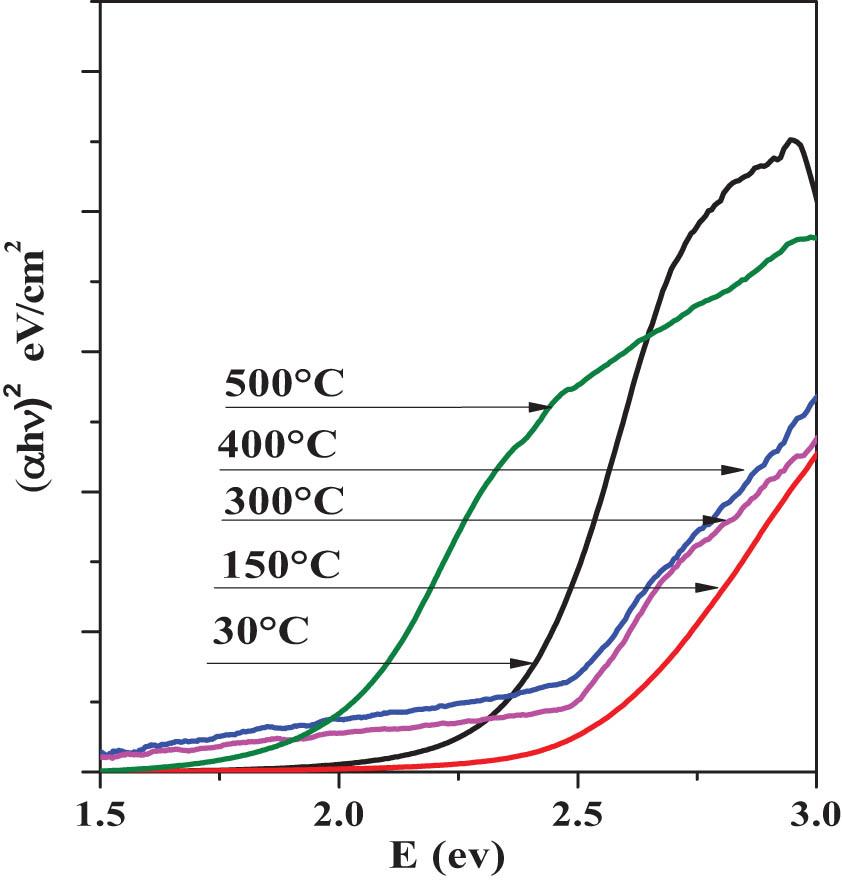
(αhν)2 vs E (hν) spectra of the 30°C, 150°C, 300°C, 400°C, and 500°C thin solid films.
Experimental values for the bandgap energy (E g) of the 30°C, 150°C, 300°C, 400°C, and 500°C samples
| Temperature (°C) | E g (eV) |
|---|---|
| 30 | 2.37 |
| 150 | 2.31 |
| 300 | 2.17 |
| 400 | 2.06 |
| 500 | 1.87 |
Figure 14(a) shows the logarithm of the absorption coefficient vs photon energy. The band tails are associated with the edge broadening exciton-phonon that can be attributed to the indirect electronic transitions in the band gap, and also the broadening reflects the disorder degree in the lattice.
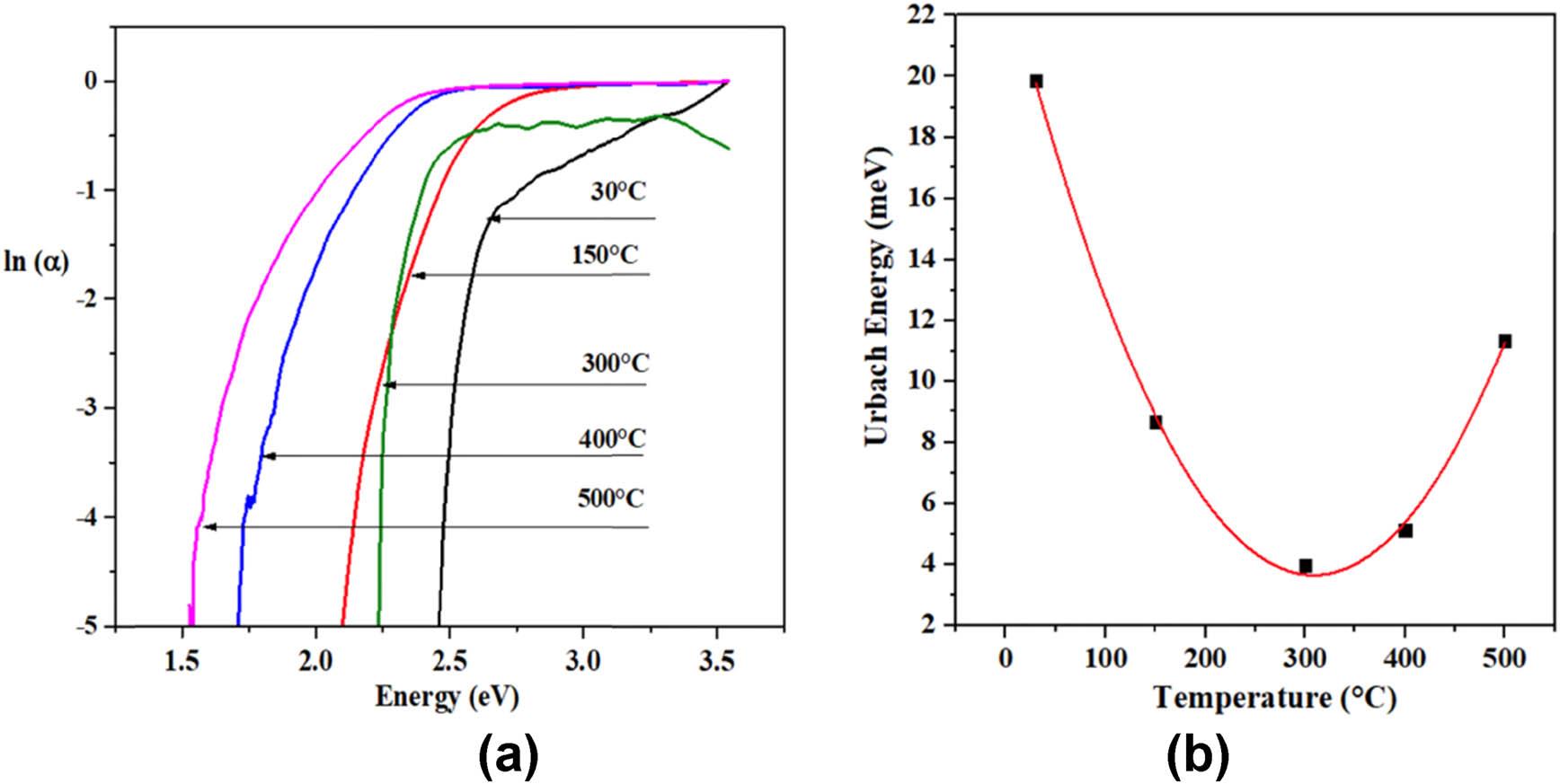
(a) Ln of the coefficient absorption, and (b) Urbach energy.
Under tensile strain, the band gap decreases, and this reduction in the band gap significantly affects the photocatalytic performance of the material. The photocatalytic activity depends on the E g and the carrier mobility.
The Urbach energy values are shown in Figure 13(b), and they depend on the structural disorder. The sample annealed at 500°C has a lower Urbach energy value, although it has been reported that high Urbach energy enhances the photocatalytic degradation [49].
The films obtained were applied to photocatalysis, under solar lighting for a total time of 80 min, and the preparation procedure is as follows:
-
Methylene blue solution is prepared at a concentration of 10 ppm, and it is applied as an organic pollutant.
-
The solution of methylene blue is added to a glass of precipitates.
-
Later, the film is immersed in the beaker with a bra that allows it to stand, maintaining constant agitation.
-
Methylene blue is sampled every 10 min to monitor the photodegradation of the contaminant.
The entire photocatalytic mechanism developed with the films is shown in Figure 14.
The catalytic activity of the films begins when the electrons absorb the radiation of sunlight as long as this energy is greater than or equal to the gap that the semiconductor has [50], allowing the electrons to have the energy needed to jump from the Valencia band (VC) to the conduction band (CB) [51], leaving in the band VB its pseudoparticle called holes and subsequently the electrons in CB react with oxygen (
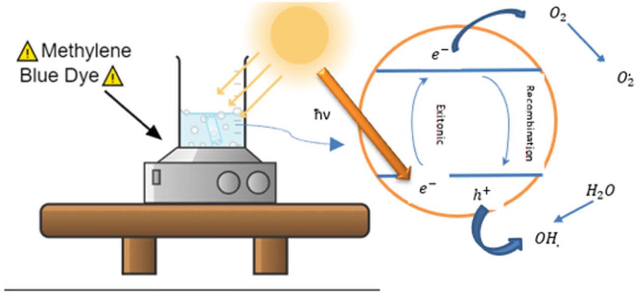
Photocatalytic process of the thin films.
The applied films have a dimension of 0.8 cm × 0.8 cm. The degradation results of all the films are shown in Figure 16. Each of those figures can be zoomed, which allows us to better observe the photocatalytic activity of each of them, but the photocatalytic activity is very small due to the low amount of material contained in thin films because it has a low surface area and because it does not have a rough surface that would function as a pollutant removal trap [57]. It can be observed that in the film with heat treatment at 500°C (10-e) has a better photodegradation result because the GAP of the material in this film is wider than that of the other films (∼1.87 eV). This allows one to make better use of the solar spectrum for generating pairs of electron-holes, which are indispensable for photodegradation. Finally, Figure 17 measures the rate of degradation of the pollutant (methylene blue) over a time of 90 min for all films. For cases of 30 and 150°C, the behavior of their catalytic activity is very similar in both films (∼8%). This is because the GAPS are very similar (∼2.37 and ∼2.31 eV, respectively). For the 300°C film, the catalytic activity efficiency is ∼11% with a gap of ∼2.17 eV; for the 400°C film, the catalytic efficiency is very similar to ∼12% (gap ∼ 2.06 eV); and for the 500°C film, a maximum efficiency of ∼14% is achieved with a gap of ∼1.87 eV.
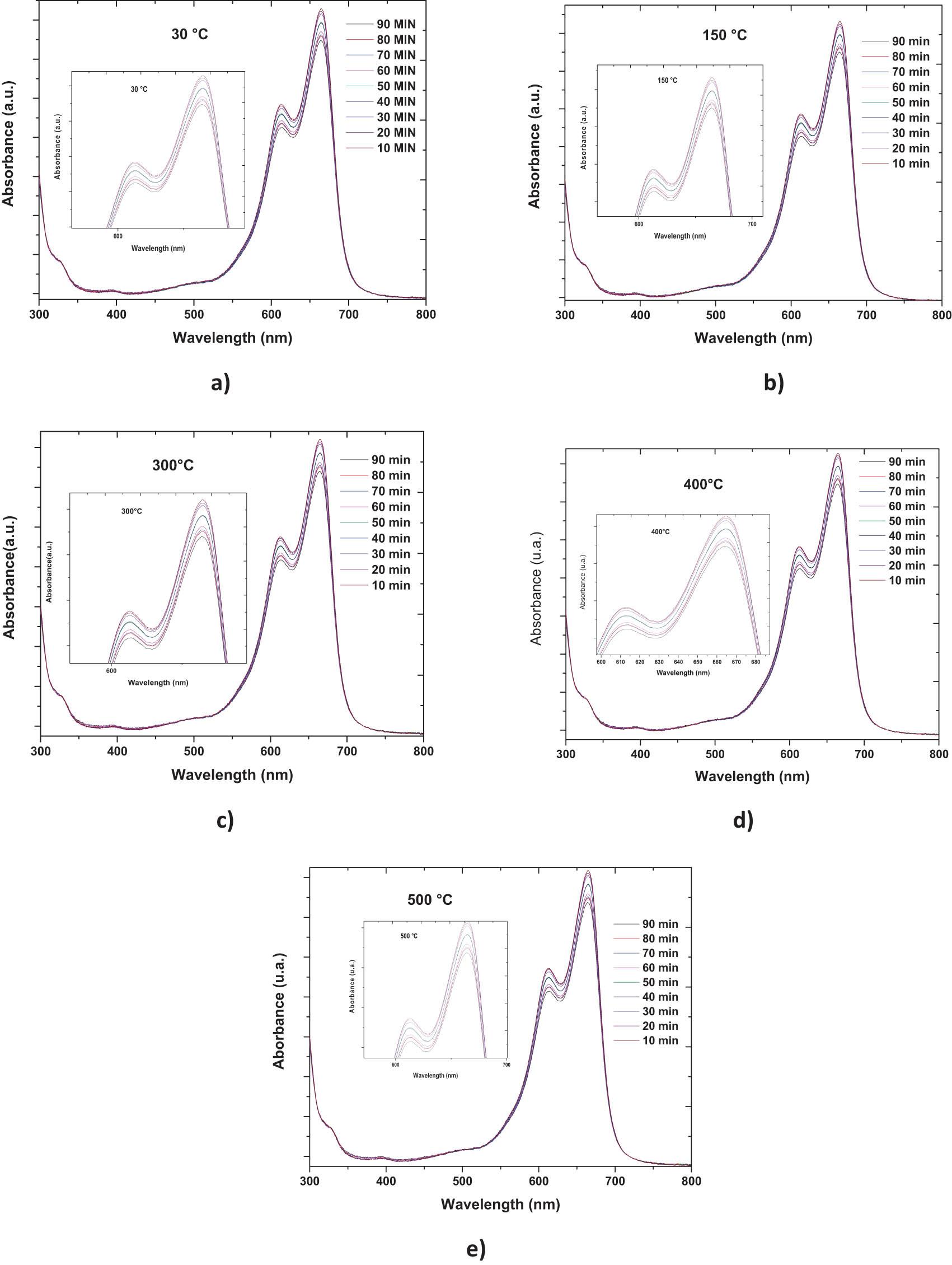
Photodegradation absorption spectra 10 at (a) 30°C, 10 (b) 150°C, 10 (c) 300°C, 10 (d) 400°C, and 10 (e) 500°C.
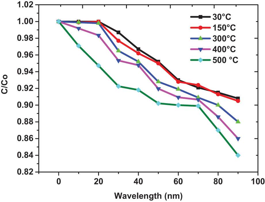
Graphical rate of catalytic degradation.
In this work, we synthesized the thin films of CdCO3 using the chemical path of CBD. The morphological, structural, and optical analyses of the films were carried out at 30, 150, 300, 400, and 500°C, as well as their conversion to CdO demonstrated in XRD. With SEM, well-formed rhombohedral figures were observed, which are characteristic of the material. Also, the atoms do not rearrange significantly during annealing, keeping the morphology relatively unchanged. Furthermore, the material is in a favorable state, and subsequent annealing may not alter its morphology significantly. With FTIR spectroscopy, we were able to observe the ionic links CdCO3, indicating the presence of the material in the films, as well as the conversion to CdO. With absorption, transmittance, and reflectance measured in films of 30°C, 150°C, and 300°C, they were observed to absorb, transmit, or reflect in the range of 450 nm, while films of 400°C and 500°C in the range of 600 nm. Tauc’s equation was used to calculate the GAP of films from ∼ 1.87 to 2.37 eV. Normalized absorption vs wavelength plots were constructed to find the transition from CdO3 to CdO at the edge at ∼1.60 eV and another at ∼1.73 eV. The films were applied to photocatalysis to study their catalytic efficiency, using methylene blue as a pollutant. A low efficiency of 8–14% in 90 min was obtained, which was due to the tiny surface of the film, as well as the surface that was not rough. These aspects will be considered for further investigation.
Authors state no funding involved.
All authors contributed to the study conception and design. Material preparation, data collection and analysis were performed by Marco Antonio Vicencio Garrido, Melissa Chávez Portillo, and Sebastian Miguel Varela López. The first draft of the manuscript was written by Marco Antonio Vicencio Garrido and all authors commented on previous versions of the manuscript. All authors read and approved the final manuscript.
Authors state no conflict of interest.
Data will be availability by request.