Figure 1
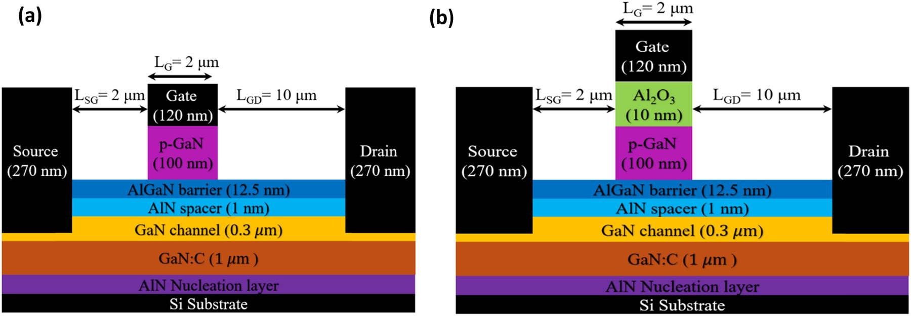
Figure 2
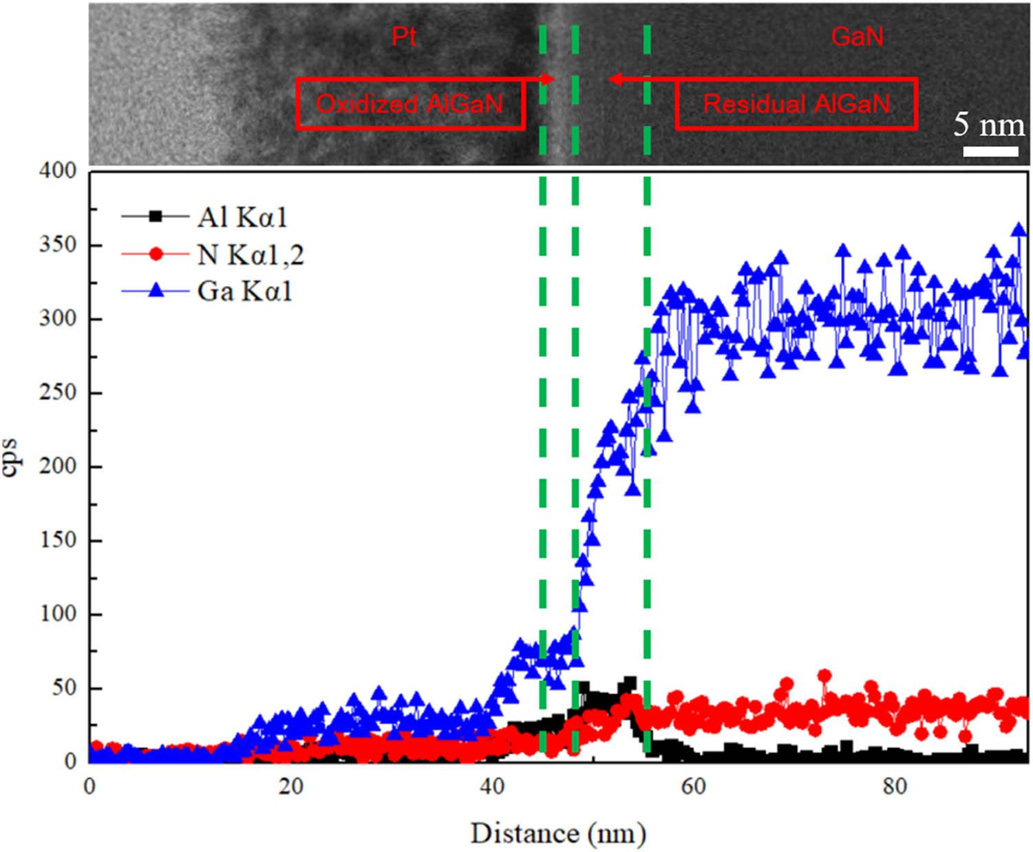
Figure 3
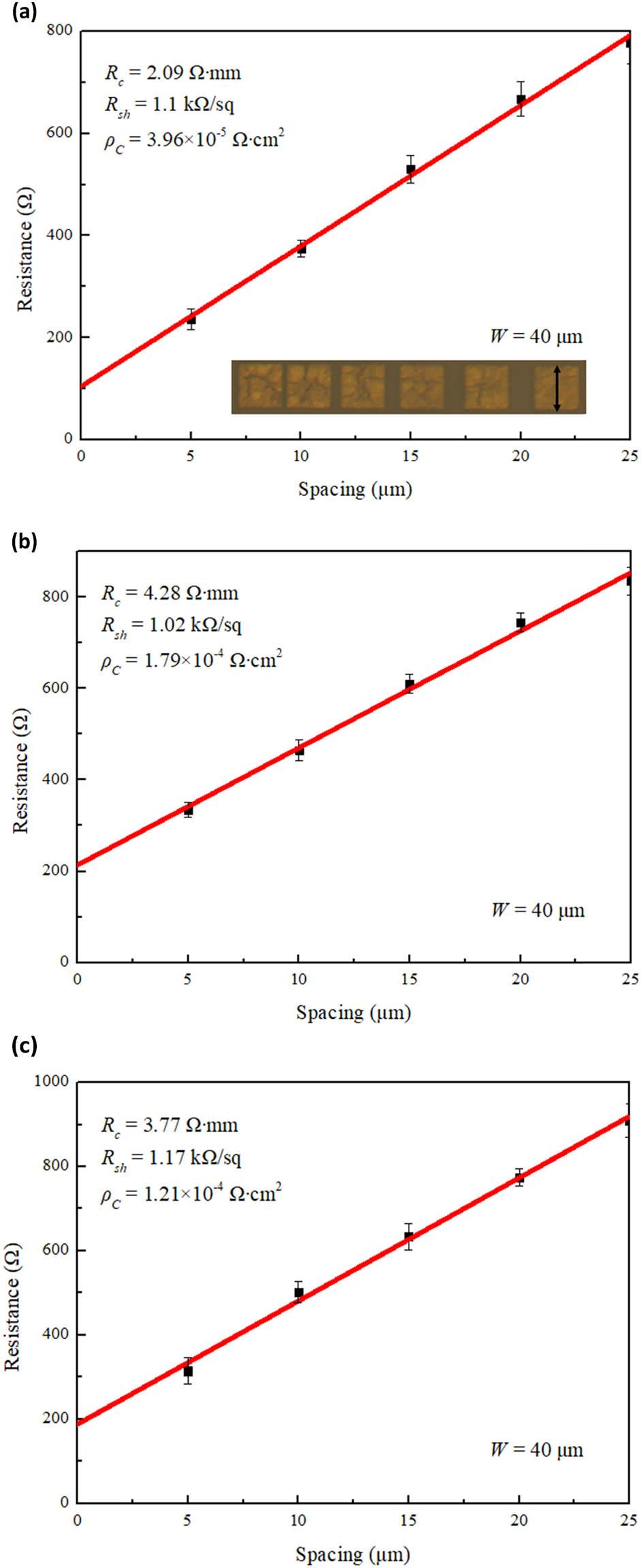
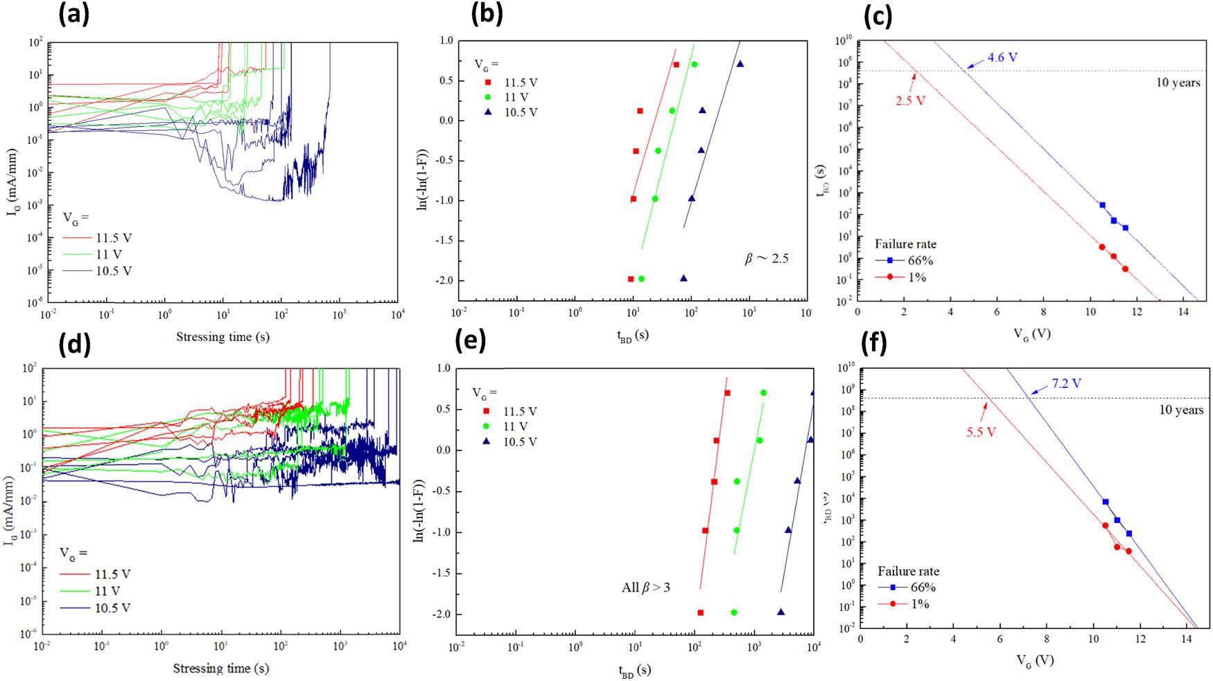
Figure 4
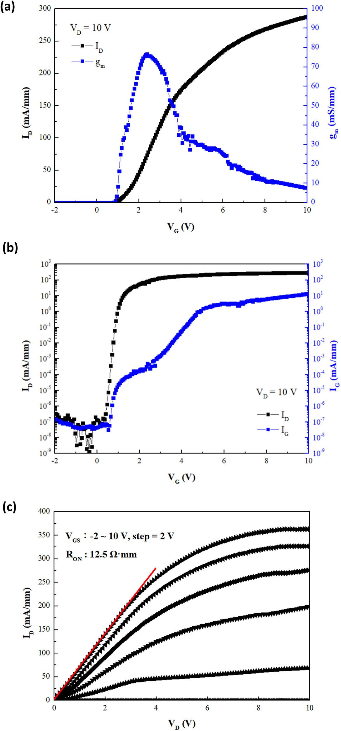
Figure 5
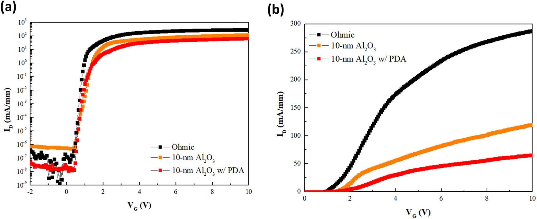
Figure 6
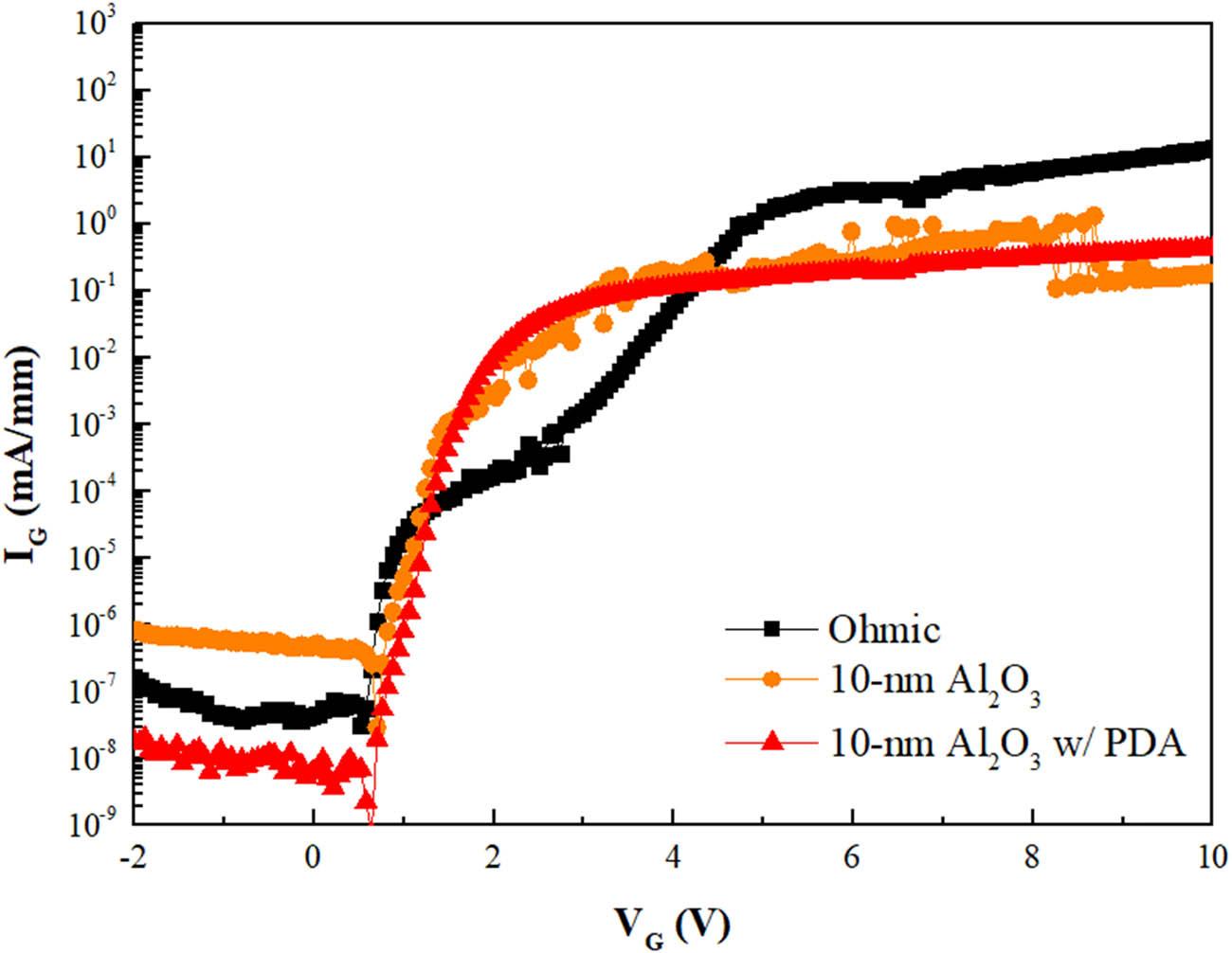
Figure 7
Comparison of switching performance parameters with other E-mode GaN-based devices_
| References | I ON /I OFF | SS (mV/dec) | V th (V) |
|---|---|---|---|
| This work (w/PDA) | 109 | 71.26 | 1.05 |
| [19] | 105 | — | 2.40 |
| [28] | 109 | 116 | 0.70 |
| [29] | 106 | — | 0.50 |
| [30] | 109 | 95 | 0.30 |
| [31] | 104 | 205 | 0.49 |
| [32] | 108 | — | 1.10 |
Comparison of typical performance parameters among the three types of HEMTs_
| Parameters | Ohmic gate | MOS-HEMT (w/o PDA) | MOS-HEMT (w/PDA) |
|---|---|---|---|
| V th (V) | 0.81 | 1.15 | 1.05 |
| SS (mV/dec) | 75.61 | 89.79 | 71.26 |
| g m,max (mS/mm) | 76.64 | 40.33 | 18.33 |
| Field effect mobility (cm2/V s) | 684 | 153 | 71.4 |
| I ON /I OFF | 2.17 × 10¹¹ | 2.48 × 10⁸ | 5.64 × 10⁹ |