I. INTRODUCTION
Recently, the vast promotion in the field of information and communication technology (ICT) such as grid and fog computing has increased the inclination of having secret data sharing over the existing non-secure communication networks. This encouraged the researches to propose different solutions to ensure the safe access and store of private and sensitive data by employing different cryptographic algorithms especially the public key algorithms [1] which proved robust security resistance against most of the attacks and security halls. Public key cryptography is significantly based on the use of number theory and digital arithmetic algorithms.
Indeed, wide range of public key cryptographic systems were developed and embedded using hardware modules due to its better performance and security. This increased the demand on the embedded and System-on Chip (SoC) [2] technologies employing several computers aided (CAD) tools along with the configurable hardware processing units such as field programmable gate array (FPGA) and application specific integrated circuits (ASIC). Therefore, considerable number of embedded coprocessors design were used to replace software based (i.e. programming based) solutions of different applications such as image processors, cryptographic processors, digital filters, low power application such as [3] and others. The major part of designing such processors significantly encompasses the use computer arithmetic techniques in the underlying layers of processing.
Computer arithmetic [4] or digital arithmetic is the science that combines mathematics with computer engineering and deals with representing integers and real values in digital systems and efficient algorithms for manipulating such numbers by means hardware circuitry and software routines. Arithmetic operations on pairs of numbers x and y include addition (s = x + y), subtraction (d = x – y), multiplication (p = x × y), and division (q = x/y). Subtraction and division can be viewed as operations that undo the effects of addition and multiplication, respectively. Multiplication operation is considered as a core operation that affect the performance of any embedded system. Therefore, the use of fast multiplier units will result in enhancements in the overall performance of the system. Recently, several solutions were proposed for multiplication algorithms while few of them were efficient [5].
A multiplication algorithm [6] is method to find the product of two numbers, i.e. P = X × Y. Multiplication is an essential building block for several digital processors as it requires a considerable amount of processing time and hardware resources. Depending on the size of the numbers, different algorithms are in use. Elementary-school grade algorithm was multiplying each number digit by digit producing partial sum with complexity of O(n2). [5] For larger numbers, more efficient algorithms are needed. For example, let a and b integers to be multiplied with n – bit equal to 1k bits, thus 1,000,000 single – digit multiplications. However, more efficient and practical multiplication algorithms will be discussed in the following subsections.
In this paper, we report on several fast alternative designs for Radix-8 based multiplier unit including: Radix-8 CSA Based Booth Multiplier, CSA Based Radix-8 Booth, Wallace Tree Karatsuba Multiplier, CSA Based Radix-8 Booth, KSA Based Karatsuba Multiplier, CSA Based Radix-8 Booth, With Comparator Karatsuba Multiplier, Sequential 64-Bit CSA Based Radix-8 Booth Multiplier, 64-bit Wallace Tree CSA based Radix-8 Booth multiplier (WCBM). The remaining of this paper is organized as follows: Section 2, discusses the core components of efficient multiplier design. Section 3, provides the proposed design alternatives of Radix-8 based multiplier, Section 4, presents the synthesizing results and analysis, and, finally, Section 5 concludes the paper.
II. CORE DESIGN COMPONENTS-REVIEW
Two operands-multiplication is a substantial arithmetic operation since it plays a major role in the design of many embedded and digital signal processors [7]. Therefore, the efficient design and implementation of a fast multiplier unit is on demand. In this paper, we propose a competitive reconfigurable multiplier design using scalable and efficient modules. Thus, the following subsections reviews the core design components for the proposed multiplier implementation unit.
A. Carry save Adder (CSA)
CSA [4] is a fast-redundant adder with constant carry path delay regardless of the number of operands’ bits. It produces the result as two-dimensional vectors: sum vector (or the partial sum) and carry vector (or partial carry). The advantage of CSA is that the speed is constant regardless the number of bits. However, its area increases linearly with the number of bits. The top view of the CSA unit along with its internal logic design architecture are provided in Fig. 1 below.
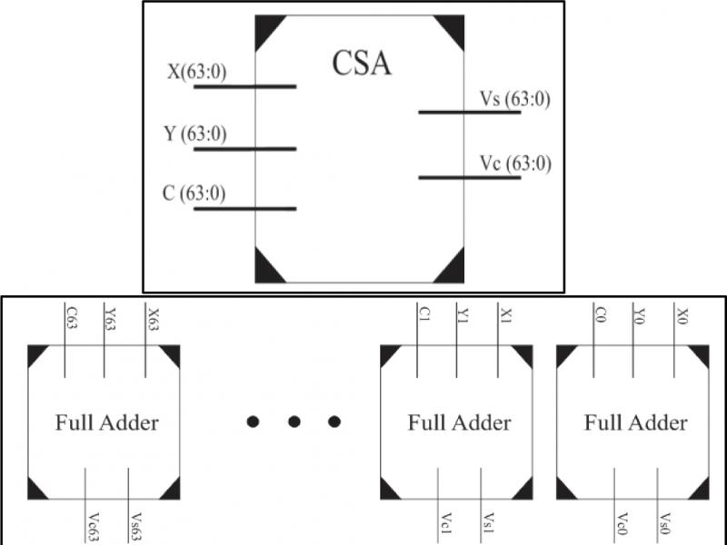
Figure 1.
Carry save Adder: (a) Top View Design (b) Internal Architecture
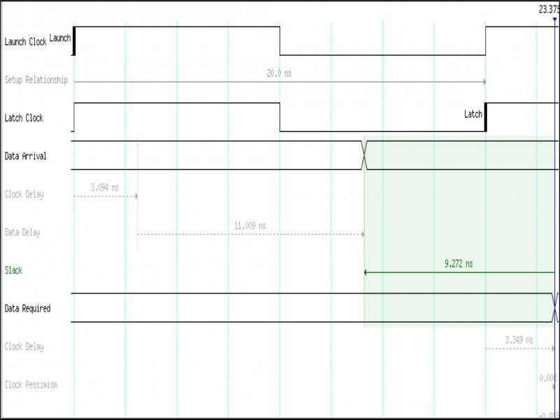
In this work, we have implemented the CSA adder using VHDL code for different bit sizes ranges from 8-bits through 64-bits [8]. The synthesize results of total delay in (ns) and area in Logic Elements (LEs) were analyzed and reported in [8] and they are illustrated in Fig. 2. These results were generated using Quartus II 14.1 software [9], simulated for Altera Cyclone IV DE2–115 model [10] and they highly conform theoretical evaluation of CSA operation since the delay time is almost equal for all bits. However, the area is almost double for each number of bits. Also, the timing estimation of 64– bits CSA was generated via TimeQuest Time Analyzer tool provided in the Quartus II CAD package. Accordingly, the critical path delay is 3.529 ns which is data arrival time while the data delay is only 2.866 ns which provide a frequency of 349 Mhz. Finally, to verify the performance of CSA, we have compared it with the well-known Carry LockAhead Adder (CLA) in terms of area and delay. CLA is a carry propagation adder (CPA) with logarithmic relation between the carry propagation delay and the number of bits in operands.
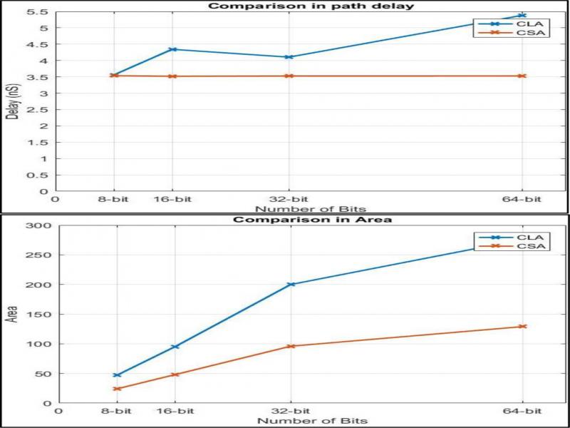
Figure 2.
Delay-Area analysis of CSA vs CLA implementations (8–64 bit)
The simulation results of both CSA and CLA is provided in Fig. 2 shows that CSA is superior in both Area and speed. It has almost a constant time delay and relatively less area than CLA. Whereas CLA time delay increases as the number of bit increases but not much as the area size.
B. Kogge-Stone Adder (KSA)
KSA is a fast two operands parallel prefix adder (PPAs) [11] that executes addition on parallelized manner. PPAs are just like CLA but with an enhancement in the carry propagation stage (called the middle stage). There are five different variations of PPAs namely: Ladner-Fischer Adder (LFA), Brent-Kung Adder (BKA), Kogge-Stone Adder (KSA), Hans-Carlson Adder (HCA), and Sklansky Adder (SkA). These adders differ by the tree structure design to optimize certain aspects such as, performance, power, area size, and fan in/out.
To verify the performance of all PPAs, we have implemented them on FPGA and the experimental results [6] showed that KSA utilizes larger area size to achieve higher performance comparing among all other five PPAs. Thus, we decided to consider KSA as our basic carry propagation adder (CPA) to finalize the redundant results and to build up many other units that are in-need for conventional adder. In short, the simulation results of [6] showed that KSA leading the other adders as it has the smallest time delay with only 4.504. This result is very useful and conforms the theatrical modeling of KSA which has the least number of logic levels. Like all PPAs, KSA functionality consists of three computational stages as illustrated in Fig. 3, as follows:
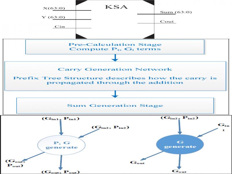
Figure 3.
Kogge Stone Adder: (a) Top View Design of KSA (c) KSA Stages (c) Group generation and propagation
Pre-processing stage: The computation of generate and propagate of each bit from A and B are done in this step. These signals are given by the logic equations: Pi = Ai xor Bi and Gi = Ai and Bi
Carry generation network: PPA differentiates from each other by the connections of the network. It computes carries of each bit by using generate and propagate signals from previous block. In this block two blocks are defined group generation and propagation (GGP), in addition to group generation only (GGO), as shown in Fig. 3. Logic blocks used for the calculation of generate and propagate bits can be describe by the following logic equations: Pout = Pin1 · Pin2 and Gout = Gin1 || (Pin1 · Gin2), Where the generation group have only logic equation for carry generation: Gout = Gin2||(Pin2 · Gin1).
Post processing (Calculating the Sum):This is the last step and is common to all adders of this family (carry look ahead). It involves computation of sum bits. Sum bits are computed by the logic given in: Si = Pi ⊕ Gi−1. The top view and the internal logic circuit is provided in the Fig. 3.
C. Fast Multi-Operands Addition
Addition operation is not commonly used to add two operands only, instead, it is more involved with multiplication and inner product computations [12]. The use of regular two operands adders leads to intermediate results before getting the last answer which affect the performance or the time delay of a system. Therefore, Multi-operand adders are manly studied to reduce this problem. Wallace and Dadda trees [13] are considered as two variations of high-performance multi-operands addition. Fig. 4. shows the dot notation to represent the digit positions or alignments (instead of using the value which is quite useful) for the use of Multi-operand addition in multiplication and inner-product computation.
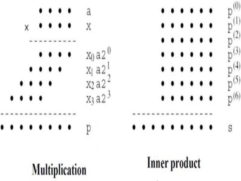
Figure 4.
Dot notation of Multi-operand addition for multiplication and inner-product computation
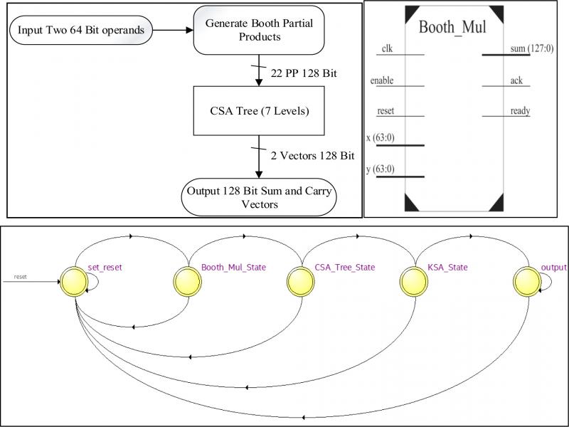
In this work, we have adopted a CSA based Wallace tree since it confirmed better operands organization to improve the total addition delay [8]. We have implemented two CSA Wallace Trees: 10-operands addition and 22-operands addition. The structure logic diagram of 10 operands is given in Fig. 5. It’s clearly seen that the Wallace tree unit is designed behaviorally (FSM is generated).
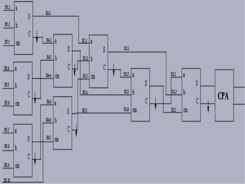
Figure 5.
Multi-operand addition for 10 operands.
D. Karatsuba Multiplier
To enhance the performance of multiplication for large operands (i.e. 1024-bit size), a re-organization process can be adopted for the multiplication operands to utilize the maximum possible parallelism to enhance the multiplication time. Karatsuba algorithm [14] is pipelined multiplication process used mainly to construct the high precision multipliers form multiple small precision multiplier blocks by exploiting the maximum available parallelism between the multiplication blocks. The basic idea of Karatsuba algorithm is illustrated in fig. 6 and Karatsuba algorithm can be defined as follows:
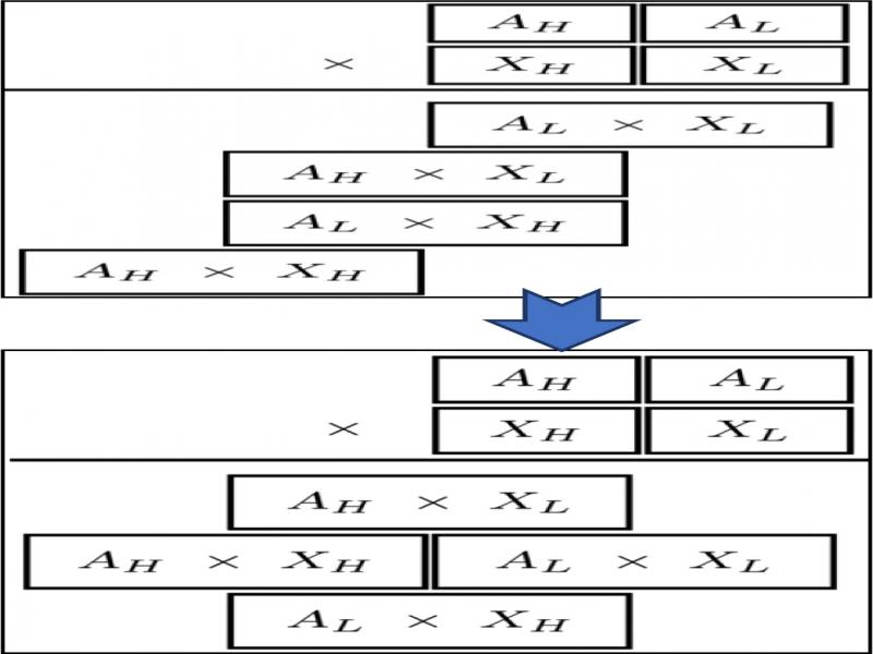
Figure 6.
Aligning Partial Products.
Let x,y be integers and B is the base (Radix_2) and m < n where n: the number of digits, then:
1) Re-write as follows:
2) Calculate Product as follows:
A more efficient implementation of Karatsuba multiplication can be accomplished as:
E. Magnitude Comparator
The magnitude (or digital) comparator is a hardware electronic device that takes two numbers as input in binary form and determines whether one number is greater than, less than or equal to the other number. Like that in binary addition, the efficient comparator can be implemented using G (generate) and P (propagate) signal for comparison. Basically, the comparator involves two 2-bits: A1A0& B1B0 can be realized by:
For A<B, “BBig, EQ” is “1,0”. For A=B, “BBig, EQ” is “0,1”. Hence, for A>B, “BBig, EQ” is “0,0”. Where BBig is defined as output A less than B (A_LT_B). Comparing Eq. (1) and (2) with carry signal (3):
Where A & B are binary inputs Cin is carry input, Cout is carry output, and G & P are generate & propagate signals, respectively. Now, after comparing equations (1) & (3), we got:
Cin can be considered as G0. For this, encoding equation is given as:
Substituting the two values from equations (5) & (6) in (1) & (2) results in:
G&P signals can be further combined to form group G&P signals. For instance, for 64-bit comparator, BBig&EQ can be computed as:
Fig 7. Shows the complete design of an 8-bit comparator as an example of this techniques where: i= 0…7, j = 0…3.
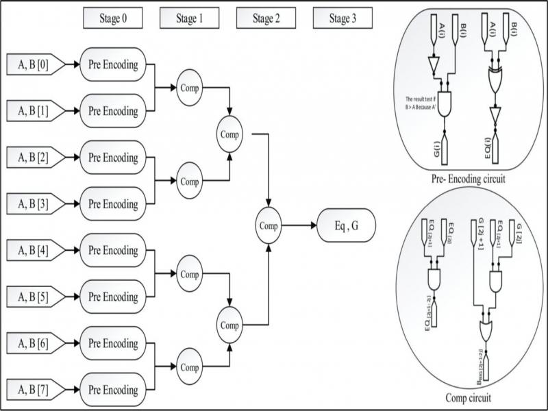
Figure 7.
The complete design of8- Bit Comparatorincluding Pre- Encoding circuit and Comp circuit
III. PROPOSED MULTIPLIER DESIGN ALTERNATIVES
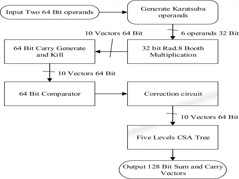
Fundamentally, multiplication operation (along with fast addition) is a significant unit in almost all cryptographic coprocessors. For instance, in the design of SSC Crypto-processor[15], the multiplication primarily used to compute the square parameter (p2), the public key (p2q) and the modulus (pq). Also, in the design of RSA Crypto-processor, the multiplier is used to compute the modulus (p.q) and the Euler function Ø(n) = (p – 1).(q – 1) [16]. One more example, is the need for fast multipliers at several computation stages of ECC cryptosystem [17]. Indeed, wide range of methods have been proposed to address the efficient design of fast two operands arithmetic multiplier. In this paper, we have spent an extensive time to design an efficient multiplier by trying several variations of different multiplier design specifications. The first design was the implementation of Radix-8 Booth Encoding Multiplier. Then, we tried many variations to employ this multiplier with different design methods. In the next subsections, we provide six design alternatives of the proposed multiplier to come up with the most cost-effective multiplier design. We finally report on the final implemented design.
A. Radix-8 CSA Based Booth Multiplier
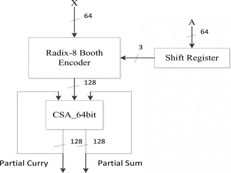
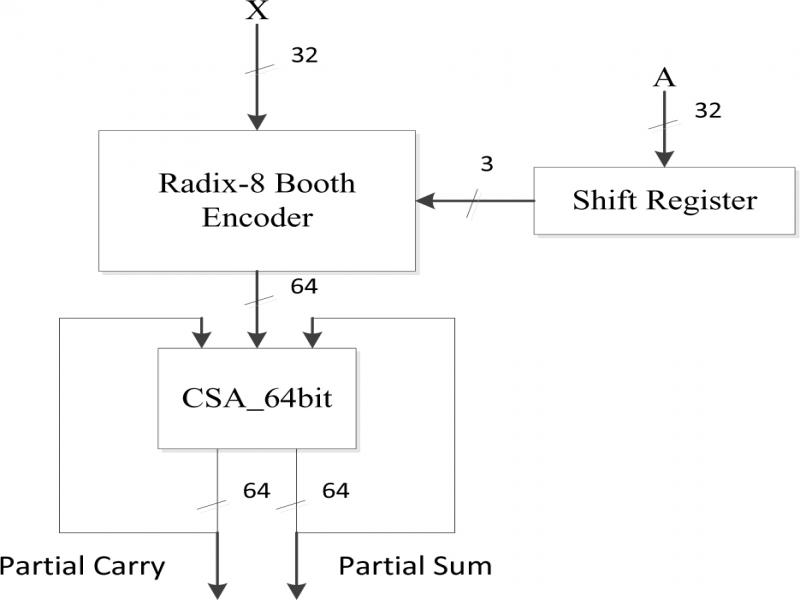
Unlike Binary radix booth encoder, Radix-8 booth encodes each group of three bits as shown in table 1. The encoding technique uses shift operation to produce 2A and 4A while 3A is equal to 2A+A. The logic diagram of implementing CSA based Radix-8 booth multiplier is shown in Fig. 8. The use of CSA provides very powerful performance with limited area cost. The partial products for radix-2 is n (where n is the number of operand bits). However, for radix 8 the number of partial products is only n/3.
TABLE I.
RADIX-8 BOOTH ENCODING.
| Inputs (bits of M-bit multiplier) | Partial Product | |||
|---|---|---|---|---|
| xi+2 | xi+1 | xi | xi−1 | PPRi |
| 0 | 0 | 0 | 0 | 0 |
| 0 | 0 | 0 | 1 | A |
| 0 | 0 | 1 | 0 | A |
| 0 | 0 | 1 | 1 | 2A |
| 0 | 1 | 0 | 0 | 2A |
| 0 | 1 | 0 | 1 | 3A |
| 0 | 1 | 1 | 0 | 3A |
| 0 | 1 | 1 | 1 | 4A |
| 1 | 0 | 0 | 0 | -4A |
| 1 | 0 | 0 | 1 | -3A |
| 1 | 0 | 1 | 0 | -3A |
| 1 | 0 | 1 | 1 | -2A |
| 1 | 1 | 0 | 0 | -2A |
| 1 | 1 | 0 | 1 | -A |
| 1 | 1 | 1 | 0 | -A |
| 1 | 1 | 1 | 1 | 0 |
| Design Solutions # | Delay (gate delay) | % Optimization | Area (# of gates) | % Optimization |
|---|---|---|---|---|
| Solution I: using KSA Adder. | 23 | +15% | 6130 | |
| Solution II: using Comparator unit. | 27 | 3712 | +50% |