

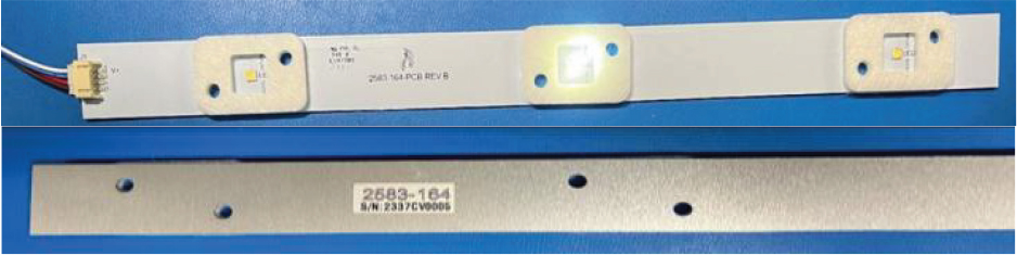
Figure 1.
A module of 3-LED (SMD 2583-164)
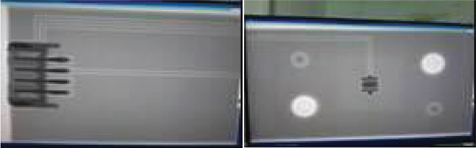
Figure 2.
X-ray image of the electrical circuit of the LED board
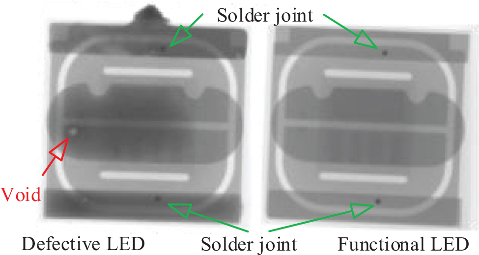
Figure 3.
X-ray image showing a defect in the LED chip
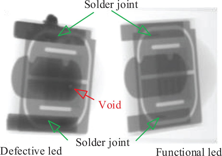
Figure 4.
Lateral X-ray image showing a defect on the LED chip
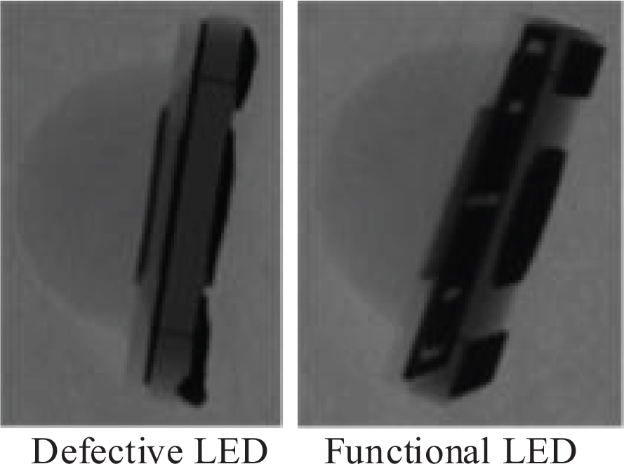
Figure 5.
X-ray image of the side view of the defective and functional LEDs
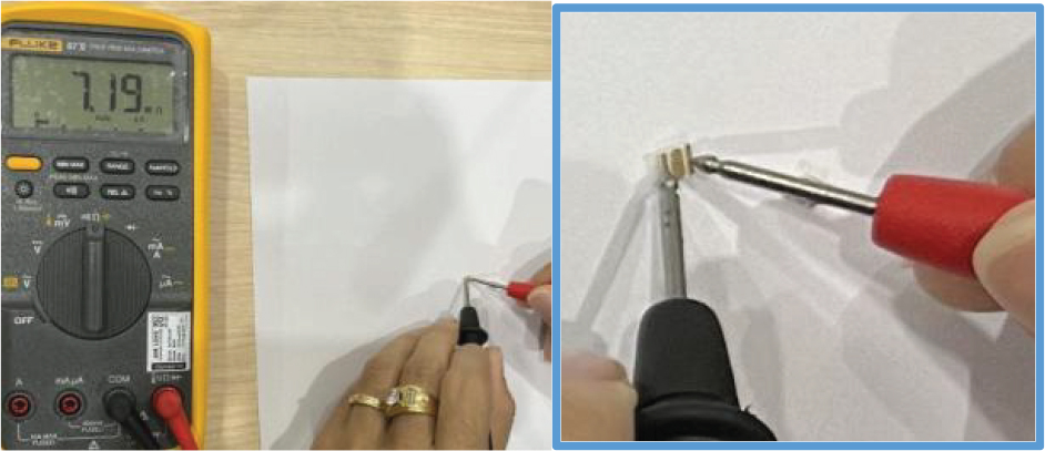
Figure 6.
Demonstration of manual resistance measurements for functional and defective LEDs
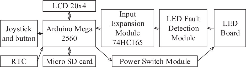
Figure 7.
Block schematic of control system
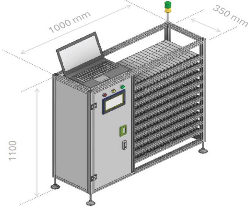
Figure 8.
Concept model of mechanical structure
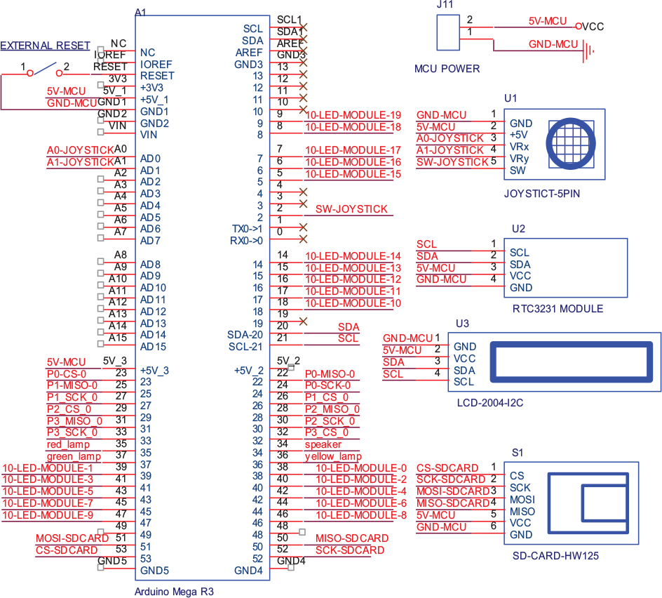
Figure 9.
Schematic diagram of control center
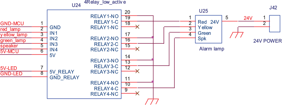
Figure 10.
Schematics of the optically isolated relay module
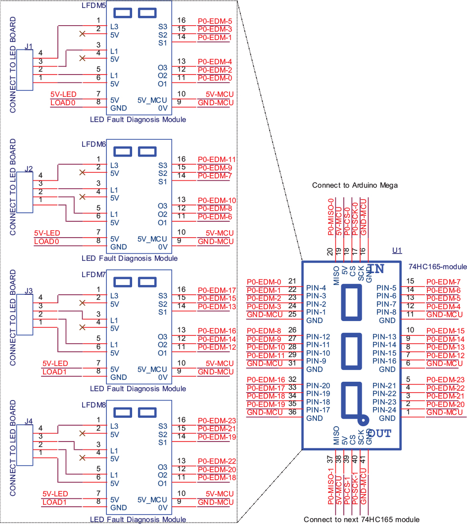
Figure 11.
Connection diagram of peripheral devices (74HC165 and LFD module)
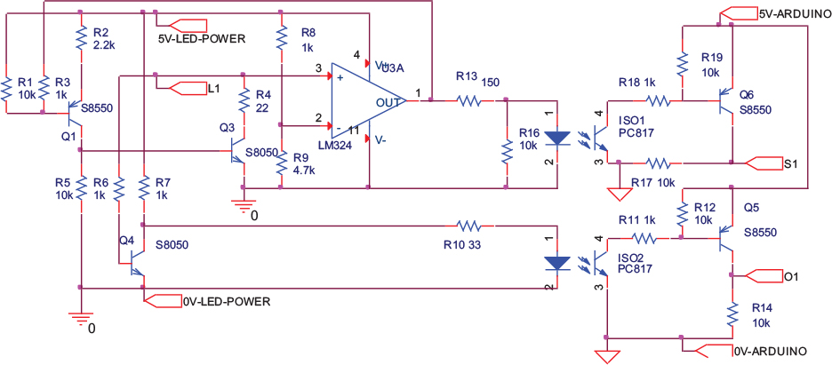
Figure 12.
Fault detection circuit of an LED
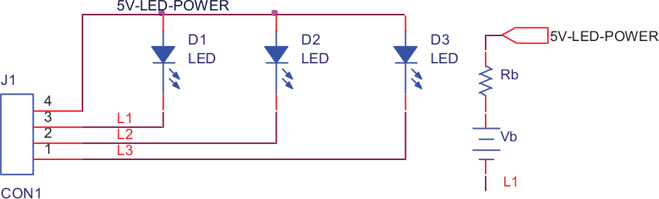
Figure 13.
(a) Schematics of a 3-LED module (SMD 2583-164), (b) the DC equivalent circuit of an LED
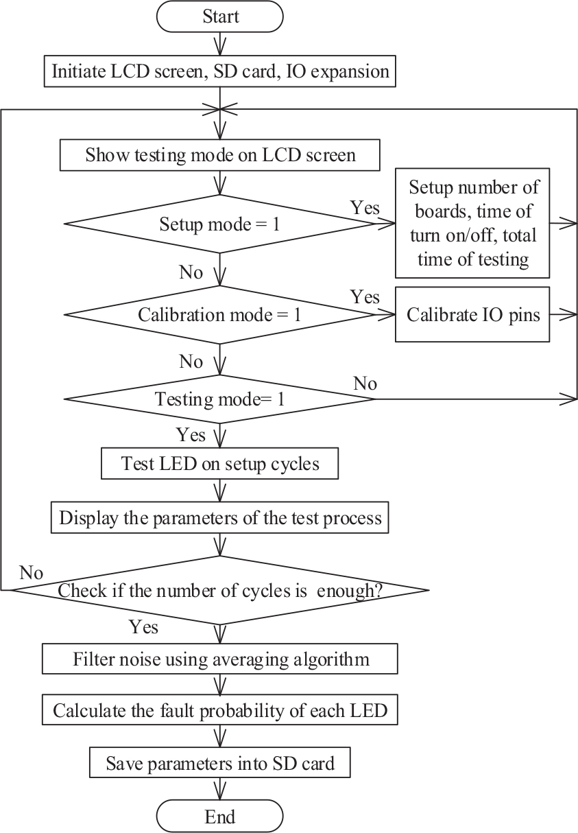
Figure 14.
Schematics of control flowchart
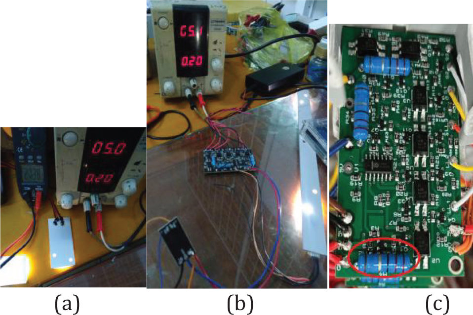
Figure 15.
Illustration of the measurement of current and voltage parameters on 1-Led model: SMD 2583-426 REV B (a), 3LED board model: SMD 2583-164 PCB REV B (b), and fault classification module (c)
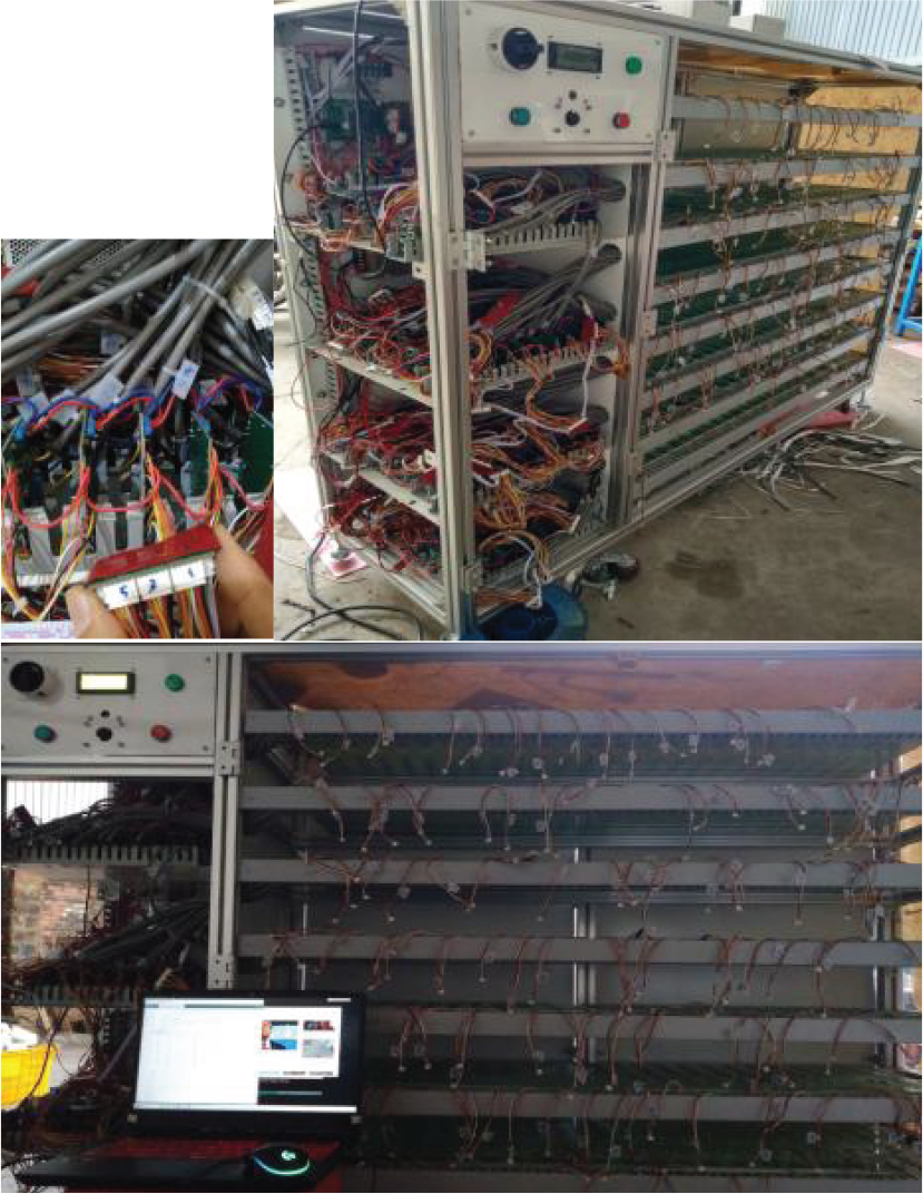
Figure 16.
LED fault tester during assembly and testing
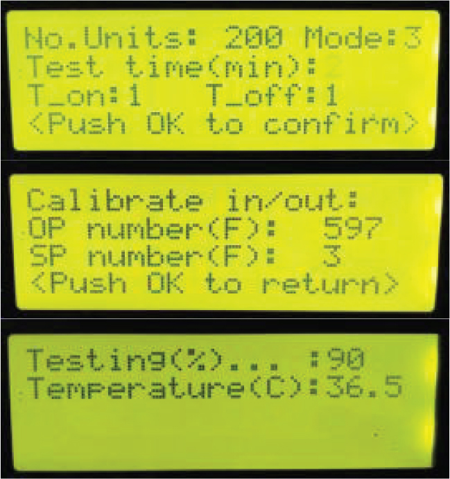
Figure 17.
Display screen of parameters
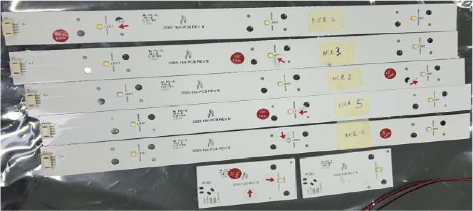
Figure 18.
Testing board samples (2583-164-PCB-REV B, 2583-426-REV B)
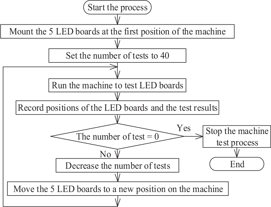
Figure 19.
Illustration of the device testing process with a small number of faulty LED boards
Table 1.
Sample of faulty LED boards (2583-164-PCB-REV B).
| N.o. Board | NCR1 | NCR2 | NCR3 | NCR4 | NCR5 | |
|---|---|---|---|---|---|---|
| LED1 | Ledl State | O | N | N | N | N |
| O pin | 1 | 0 | 0 | 0 | 0 | |
| S pin | 0 | 0 | 0 | 0 | 0 | |
| LED2 | Led2 State | N | N | S | O | S |
| O pin | 0 | 0 | 0 | 1 | 0 | |
| S pin | 0 | 0 | 1 | 0 | 1 | |
| LED3 | Led3 State | N | O | N | N | N |
| O pin | 0 | 1 | 0 | 0 | 0 | |
| S pin | 0 | 0 | 0 | 0 | 0 |
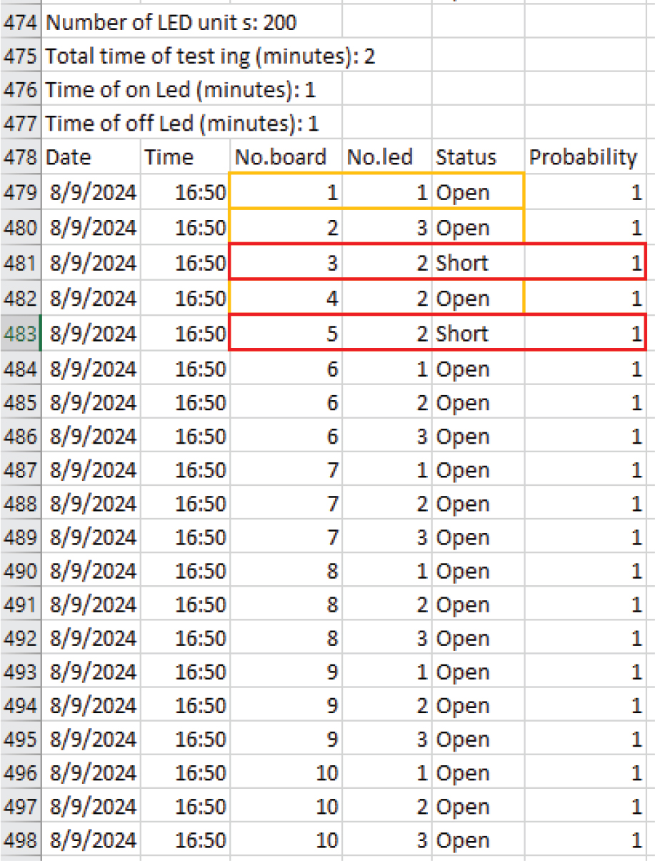
Figure 20.
A report sample of the testing result