
Overview
Introduction
Simulation methods are a fundamental component to understand, validate or even enhance experimental results. Often applied modelling is focused on either predicting the behaviour of experimentally fabricated devices [12] — aiming for a more efficient fabrication process — or directly validating the results by fitting experimentally measured parameters with the simulated values [34]. For optical measurements, more specifically, spectrophotometry, where the core results are the reflection, transmission and absorption of planar stacks of layers, matrix-based methods constitute effective and accurate approaches to model these properties [5]. Here, the scattering matrix method (SMM) is often a preferred approach as it provides more stable calculations, in contrast to other techniques, such as the transfer matrix method (TMM), that can provide faster calculations [5]. This is a consequence of the SMM, in contrast to the TMM, considering the proper direction for mode propagation inside the layers stack, thus avoiding the wrong superposition between transmitted and reflected waves between layers. In this case, we chose to use the former since a stabler method is preferable for graphical applications. Nevertheless, due to the significant computational improvements in the last decade, the SMM can still be solved fast enough for the generality of cases, with the here-calculated results for broadband simulations and a stack of 3 layers tacking less than a few milliseconds.
In addition to educational/learning uses, the applications of the scattering matrix method branch out to many different areas, namely those involving light interaction with layered devices as is the case of optoelectronic technologies. One such example, that is also a focus of this work, is thin-film solar cells. Often here, the determination of the light absorption properties of the device is fundamental to accurately determine its photovoltaic efficiency. For instance, determining the regions of highest/lowest absorption can often suggest how to improve the absorption in the active (photocurrent generating) layer(s) of the device. Beyond that, this method can also be used for a fast screening of possible layer thicknesses to determine the best performing set. Similarly, another important application is the determination of the thicknesses of simple stacks of layers by fitting with spectrophotometry-acquired spectra. Here, the SMM can be used as a comparison point to other experimental measurements. Different measurements giving similar values is important for a proper validation of the results.
In this work, we developed an easy-to-use open-source graphical interface (https://github.com/perspe/Scatmm) for the scattering matrix method, that can be forthwith installed and used to determine the reflection, transmission and absorption of an arbitrary stack of isotropic material layers. The program also has an added feature, often of the interest of the optoelectronics community, of calculating the absorption a particular layer of the stack. For instance, in solar cells this can be important to determine the useful absorption in the active layer(s), excluding the parasitic absorption in other layers (e.g. selective contacts) of the devices thus allowing the calculation of the photocurrent generation in thin-film solar cells. Other notable applications are the study of distributed Bragg reflectors for creating optical filters.
The user-friendly open-source nature of SCATMM also eases its coupling with different complementary tools in view of exploring prospective synergies for various technologies. As an example, when working with other specific programs more focused on the electric transport properties in solar cells, such as SCAPS-1D [6], AFORS-HET [7], among others, one could make use of importing the photo-generation profile determined with SMM, having higher accuracy in simulating the optical (wave interference) effects at play within multilayered structures, to then output the full optoelectronic response of the devices.
Here, we describe the core usage process of the program as well as several comparisons against other well-established methods to validate the implementation of the model. Lastly, we show a case application by fitting and comparing to experimental results.
Implementation and architecture
The core method used in this program is the semi-analytical 1D scattering matrix method (SMM), which can be applied on an arbitrary multilayer stack considering that each layer in the stack is infinite in the plane normal to the incidence direction and is built from an isotropic linear material. This program was built considering application to optoelectronic devices such as solar cells (where most materials behave isotopically). Hence, the added complexity of calculation and interface implementation of the method for non-isotropic materials was not considered justifiable. Nevertheless, it is a possible improvement for future iterations of the software.
The Scattering Matrix Method
The theoretical development of the semi-analytical method used in this work is mostly based on the work by Rumpft et. al., [5] with the aforementioned approximation to isotropic materials.
The core idea of the scattering matrix method is to create a matrix for each layer in a multilayer stack that contains the information relative to light’s propagation inside that layer. This matrix can then be cascaded to connect various layers and thus determine the total reflection and transmission from the layer stack. The concept is shown in the schematic of Figure 1, where the layer stack is defined by the S1–S5 scattering matrices. These will then be cascaded to create the composite matrix SDevice as detailed further below. Above and below the multilayer region (relative to the incidence direction) there is also the reflection and transmission regions, respectively, that define the materials surrounding the device. These are often considered to be vacuum/air with fixed refractive index n = 1, although there are some situations, as explored in Section 6, where changing these n values can help stabilize the simulation.
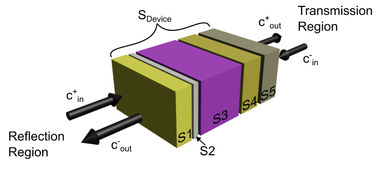
Figure 1
Visual representation of the layer cascading process in the SMM. The schematic is defined by three main regions. First, the reflection region above the stack, assuming incident light comes from this side, where the front surrounding medium and incident light properties are defined. Second, there is the transmission region, right-side, that defines the rear surrounding medium. Here, c-in is 0 (no rear incident light). The defined object layers are in between these regions, represented by the S1–S5 scattering matrices. The composite scattering matrix for the full layer stack is termed SDevice.
Firstly, this method assumes a planar wave for the incident light directed along the z axis, and that the layers are infinite in x and y dimensions (thus the materials only change in z). Considering that, it is possible to convert Maxwell’s equations into the matrix equation shown in Equation 1, where Ex, Ey are respectively the x and y components of the electric field, Hx and Hy are x and y components of the magnetic field, and kx and ky are the x and y components of the wavevector inside a particular layer. Here, the tilde (~) indicates that these values are normalized, to maintain both the E and H fields at the same order of magnitude, to improve the general accuracy of the method. Lastly, εr and μr are the relative permittivity and permeability of the layer material.
The solutions, Ψ(z’), are thus given as follows (Equation 2), where λ is the incident light’s wavelength, c+ and c- are the propagating eigenmodes in a particular layer and W and V the eigenvector matrices with the solutions for the electric and magnetic fields. In this case, due to the isotropic approximation, both W and V are the identity matrix.
The scattering matrix can thence be built here by applying the boundary conditions to the interface of each layer by matching the eigenmodes in each side (Equation 3). This setup is also shown via the schematic in Figure 2 (b), where Ψ is matched at each layer interface to guarantee the proper mode propagation between layers. The scattering matrix elements are also shown visually in Figure 2 (a) (left-side schematic). Basically, each component represents a general property of the simulation setup. For instance, the S11 element is often used to indicate the total reflection of the layer, while S21 usually represents the total transmission.
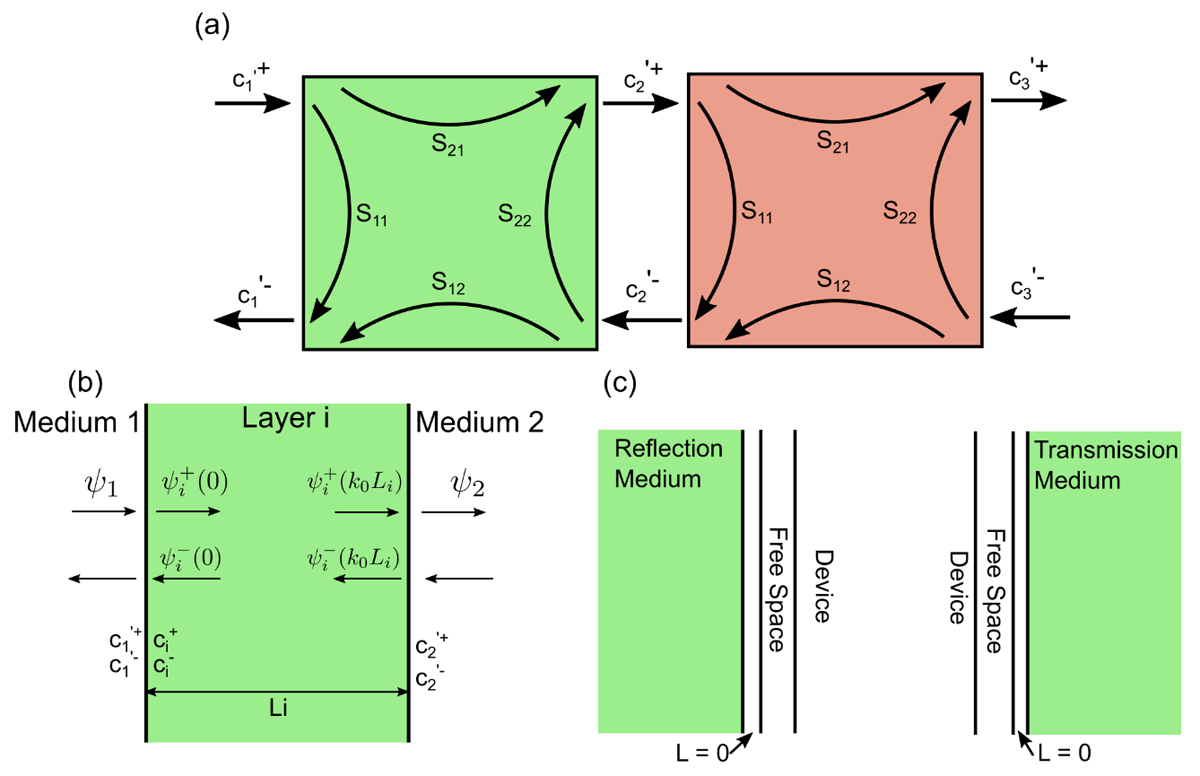
Figure 2
Schematic representation of different steps in the formulation of the scattering matrix method. (a) Schematic showing the scattering matrix elements, S11, S12, S21 and S22, as well as the mode coefficients, c, that describe the internal interaction of light with a specific layer. The schematic also shows how the mode coefficients can be used to connect different layers. (b) Schematic showing the solutions to the matrix-wave equation, where ci+/- are the mode coefficients for layer i and ϕi the solutions for a particular layer. (c) Schematic defining the scattering matrices for the reflection (left) and transmission (right) regions. Here, we defined the medium for the scattering matrix to be vacuum.
Also, a notable simplification developed by Rumpf [5] is the process of surrounding each layer by a 0-thickness layer of vacuum. This is a fundamental step as it allows for the calculation of a scattering matrix that is independent of each surrounding layer, thus greatly simplifying the complexity of the calculations. The resulting scattering matrix elements can then be calculated from Equations (4), where and , and the subscript 0 represents the properties for free space.
The scattering matrix provides thus all the information regarding the propagation of light in a particular layer. At this point it is then necessary to connect the matrices for different layers and thus obtain a final global matrix (SDevice) that incorporates the reflection and transmission information for the system. For that it is necessary to use the Redhaffer star product between two scattering matrices (A and B). This product is summarized in the equations bellow, and the schematic in Figure 2 (a) shows visually the connection process.
After cascading the scattering matrices of all the individual layers (creating SDevice), it is still necessary to add the effect of the surrounding media. For that, two different scattering matrices are developed (following the schematic of Figure 2 (c)). Essentially, in the reflection region above the stack (left-most schematic of Figure 2 (c)) the layer scattering matrix and the right-side material are considered to be vacuum with 0 thickness, to properly connect with the layer system, while the left-side material has the properties of the surrounding medium, thence attaching those properties to the layer system. The transmission-side scattering matrix is essentially the opposite of the reflection scattering matrix.
After cascading all the components of the scattering matrix (SGlobal), it is possible to connect the reflection (ref), transmission (trn), and incidence (inc) eigenmodes via Equation 6. In this case, incidence is only considered from the left, such that in the end and .
From the transmission and reflection eigenmodes it is possible to determine the transverse (x and y) electric fields, and from there the longitudinal component of the electric field (z). With all these properties calculated, it is possible to determine the total reflection and transmission of the layer stack, as described in Equations 7, where the superscripts ref and trn indicate the specific properties for the reflection and transmission regions, respectively.
Figure 3 shows the pseudo-code implementation of the scattering matrix method. The full code is available in [8]. Essentially, the method has 3 main steps as described in Figure 3. Firstly, there is the initialization of all the components necessary for the calculations, such as the free space parameters, the transverse wavevectors (transverse vectors, orthogonal to the incident light), and initialization of the global scattering matrix. Secondly, the algorithm goes through each layer in the stack, determines the scattering matrix for that layer and updates the global scattering matrix. Lastly, the transmission and reflection regions are connected to the global scattering matrix and, with the source information, the transmitted and reflected electric fields are calculated, and thence the total transmission and reflection of the stack.
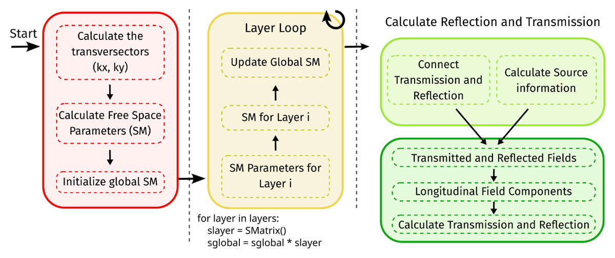
Figure 3
Pseudo-code schematic indicating the three main implementation sections for the scattering matrix (SM) method code. In red, there is the initialization section, where the incident light information is determined and the global scattering matrix (SGlobal) is initialized; the second section is the layer loop, where the scattering matrix for each layer is determined and the global scattering is thus updated; the last section is the finalization step, where the transmission and reflection region information is added followed by the determination of the transmission and reflection.
Material Optical Models
The scattering matrix method requires detailed optical information, specifically the complex refractive index spectra, of the constituent materials. To simplify access to this information, the SCATMM program includes an internal index database featuring common materials used in photovoltaic-related technologies. These materials were mostly sourced from the well-known web database Refractive Index [9], but the internal database of the program can be easily expanded by adding other materials as needed. The only limitation to consider here is that each refractive index spectrum is defined within a certain wavelength range, according to the data provided to the program, and thus simulations are only computed inside those spectral limits.
The main internal database control window is shown in Figure 4 (top window). This window is subdivided into 3 main panels. Firstly, the control database buttons (1), where it is possible to add new materials, either from a datafile (“Add Materials”) or from a set of properties from a well-known empirical dispersion formula (“Add from Formula”). Secondly, there is the actual database information (2), where all the stored materials are shown. Here, the three main columns summarize the most relevant properties, namely the name of the material and the minimum and maximum wavelength limits. These limits are important to consider during the simulations, as they set the upper and lower bounds for the spectral range allowed in the simulations. Lastly, there is also a panel where it is possible to preview the spectra of the real and imaginary components of the materials’ refractive indices (3). To preview the material, it is only necessary to drag and drop it from panel (2) to (3). The displayed material(s) can then be controlled by right clicking in section (3) and deselecting the unwanted materials.
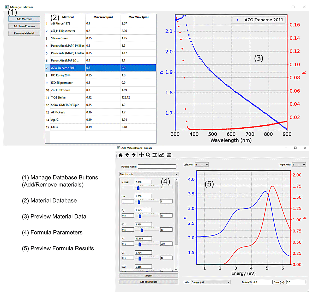
Figure 4
Graphical visualization of the database of experimentally obtained refractive index spectra (top), as well as of the applet to add modelled spectra (bottom) windows. The database window is divided into 3 main panels; the manage database buttons (1), the materials database (2) and the graph to preview the refractive index data (3). The add formula window is divided into 2 main panels; the model parameters control (4) and the graph to preview the resulting refractive index with the current settings (5).
One of the allowed methods to add materials’ indices is via pre-existing analytical dispersion formulas from well-known theoretical models. Figure 4 (bottom window) shows the interface to build these materials. This window has two main panels. First, the formula control (4), where it is possible to select the desired formula and choose the values for each of its parameters. The currently provided models are the well-known Tauc-Lorentz [1011], New Amorphous [12], Cauchy, Cauchy absorbent and the Sellmeier absorbent [13], which are commonly used formulas. We also note that a possible future improvement is the addition of user-defined formulas, to enable creating fully customisable complex refractive index functions for the materials. In panel (5) it is also possible to directly preview in real time the resulting refractive index spectra from the formulas’ settings.
Main Interface
The major advantage for this software is the easy-to-use/easy-to-install and open-source graphical interface, that does not need any code knowledge to be used. Therefore, such tool can be employed for instance by educators, researchers and product developers without requiring a priori programming expertise.
Figure 5 shows the current appearance of the graphical interface with all the core elements highlighted in different colours. Firstly, in red, the interface panel is where the properties of the layer stack and surrounding media (e.g. air) are defined. Each layer is defined by the widget highlighted in the dashed red line. This element has different important aspects. From left to right, the blue region indicates the enabled drag-and-drop feature, which allows for the rearrangement of the layer stack by simply dragging and dropping the layer widget in the desired position relative to the other widgets. Then the “Abs” checkbox indicates the option to display the layer absorption. By clicking this checkbox, the absorption of that layer will be shown in the plot to the right (blue panel). The following drop-down menu shows all the materials imported to the database, so that a specific material can be chosen for a particular layer. The next label is the element where the layer thickness is introduced, in units of nanometer (nm). The last button (the cross icon) simply allows to delete that layer. After defining the properties of each layer in the stack, the reflection and transmission elements, — top and bottom part of red panel — allow for the definition of the real (n) and imaginary (k) components of the refractive indices of the surrounding media,1 respectively in the illumination and shadow side of the stack. This is often useful when fitting the thickness of a single layer atop of a substrate (e.g. glass), as performed in the following Section 6. Due to the large substrate thickness relative to the wavelengths dimension, it is accounted for as an infinite medium.
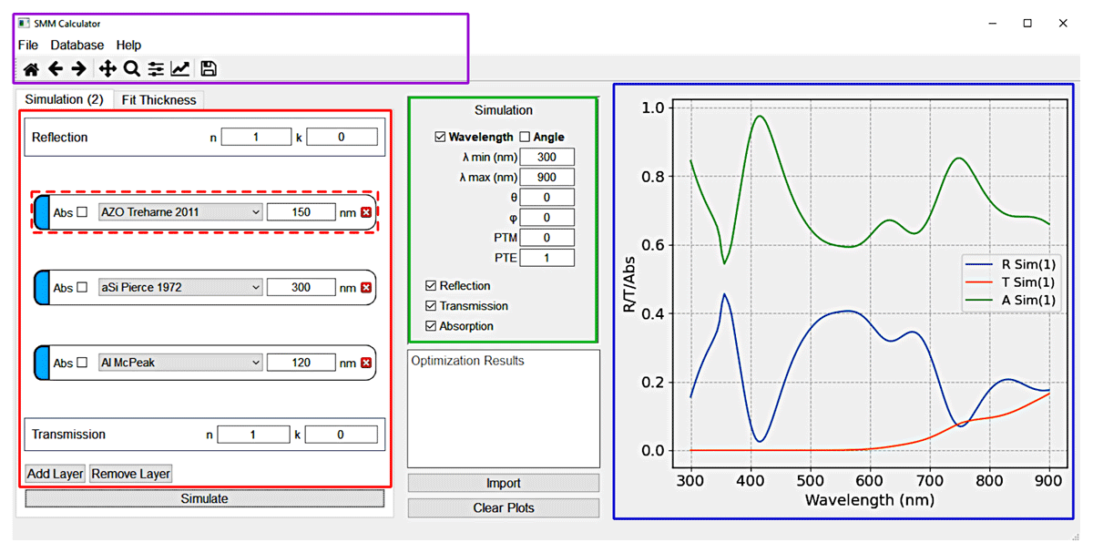
Figure 5
Main interface panels of the SCATMM program highlighted in a different colour. The purple panel is the main menu, including access to the database, help and the session-stored simulations. The red panel is the core element of the interface where the layers and surrounding materials are defined. The green panel is where the simulation configuration is defined. The blue panel is the preview region, where the simulated results are shown.
The green panel displays the simulation properties. Here it is possible to define all the elements for the computations such as the wavelength range (λmin and λmax), the incident polar (θ) and azimuthal (ϕ) angles, and the normalized components of the polarization elements (TE for transverses electric and TM for transverse magnetic). The last checkboxes tell the program which quantities to plot (between reflection, transmission and absorption).
To the right, highlighted in blue is the panel showing the desired simulated plots. The displayed spectra can be cleared by using the “Clear Plots” button bellow the green simulation setup panel. It should be noted that the program does have an internal storage (for each session) that keeps all the simulations, unless otherwise cleared, so that clearing the plots only erases the information from the profiles on the right. To access these stored simulations, it necessary to go to the “File” menu — in the purple highlighted panel — and choose “Export”. In this panel one can define additional basic properties — “Properties” section — such as the number of wavelength points for the simulations. It is also possible to access the help information — in the “Help” menu — and the database — in the “Database” menu.
After everything is properly setup, the “Simulate” button bellow the red panel is pressed to run the program.
Quality control
An important step in the implementation of any method is the validation against other well-established methods in the literature. For this case, we chose to corroborate against the commercial Finite differences time domain (Lumerical FDTD) solver from Ansys™, as it is currently one of the most widely used numeric mesh-based programs for optical simulations in optoelectronics [1415161718].
The validation is divided into 2 main parts. Firstly, there is the simple simulation with normal incidence of a basic perovskite solar cell (PSC). A standard PSC structure was chosen as test bed since this is currently one of the most researched thin-film photovoltaic technologies [1920], and this program was built with the application to solar cells in mind. Moreover, this also represents a complex comparison case as it is a multilayered structure composed of materials with quite distinct optical properties. Still, as previously mentioned, this method is applicable to the optical modelling of any isotropic stack of planar layers.
The inset in Figure 6 (a) shows the stack of layers used for the PSC with their respective thicknesses, which are common values used in the literature [19]. The thickness of the perovskite layer is treated as a variable, changing from 300 to 500 nm. The calculation was also made for two different scenarios. First, for the total absorption of the device, shown in Figure 6 (a), and secondly for the absorption only in the perovskite layer, presented in Figure 6 (b). This later result is particularly relevant for solar cell simulations, as only the active layer’s absorption — perovskite in this case — contributes for photo-carrier generation, thus it ignores all the other parasitic absorption from the remaining layers. Comparing the profiles in Figure 6 (a) and (b) it is evident that, particularly for wavelengths bellow 400 nm and above 800 nm, there is some degree of parasitic absorption mostly occurring in the electron (ITO) and hole (Spiro-OMeTAD) selective transport layers, respectively. From both profiles there is an excellent matching between the numerical and our semi-analytical results, thus reinforcing the validity of the method implementation. As such, the SCATMM program can conversely be employed as an easy-to-use validator for FDTD solvers (or any other numeric method), particularly to guarantee proper settings of the simulations (e.g. mesh properties and boundary conditions).
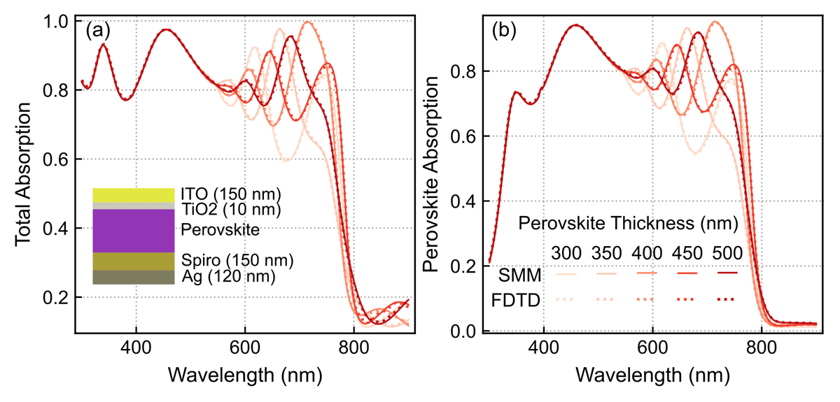
Figure 6
Comparison of computed absorption spectra between the FDTD (dotted lines) and SMM (full lines) methods, considering normal light incidence on a perovskite solar cell (PSC) with changing perovskite thickness from 300 to 500 nm. (a) Total absorption in the PSC multilayer structure (depicted in inset); (b) Useful absorption only within the perovskite layer that generates photocurrent.
For the second comparison case, we studied the behaviour for changing incidence angle, for both transverse magnetic (TM) and transverse electric (TE) polarizations (Figure 7 (a) and (b), respectively). This study adds further validation beyond normal incidence whose inherent simplifications can sometimes hide certain code/method mistakes. For simplicity, only the total absorption of the PSC structure with 500 nm perovskite thickness was considered. It can be seen again that there is an excellent agreement between the results of both methods. Nevertheless, it is noteworthy that the FDTD results do require some careful adjustments of the model settings, as there are several limitations rising from its numerical and time-domain nature. Particularly, at higher incidence angles, the perfect matching layer (PML), which is the layer responsible for absorbing all incident radiation at the limits of the FDTD simulation, can underperform and thus negatively impact the results.
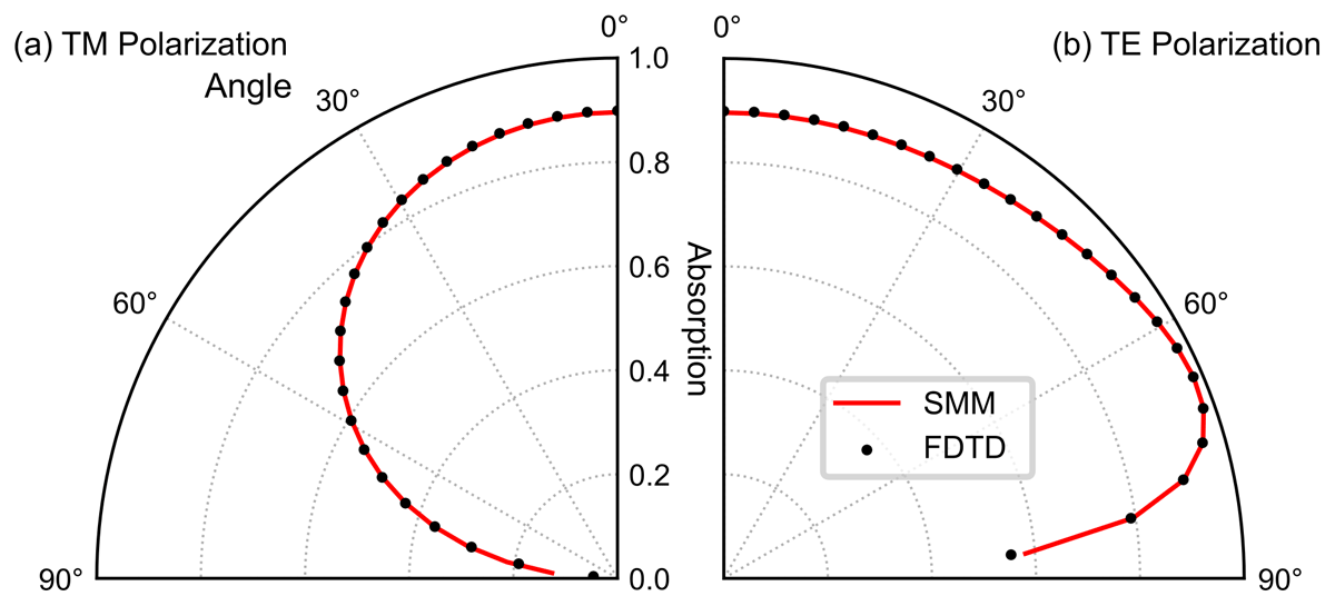
Figure 7
Comparison of angular absorption profiles between the SMM and the FDTD method, considering light incident at different angles on the same PSC structure of Figure 4 with 500 nm perovskite thickness. The dotted lines indicate the FDTD results and the full red lines the SMM results. (a) Results for the transverse magnetic (TM) polarization; (b) results for the transverse electric polarization (TE).
Experimental validation
An example of application of this method, as indicated previously, is the determination of the layers’ thickness when fitting against spectrophotometry measurements. For that, the main aspect to be matched is the spectral positions of the interference peaks from the transmission and/or reflection data (as indicated by the vertical helper lines in Figure 8 (a)). Generally, when the interference peaks from the simulated and experimental spectra are at the same wavelengths, the simulated layer(s) thickness(es) should be very close to the experimentally observed ones. Notably, such exercise can further contribute to demonstrate the validity of the model.
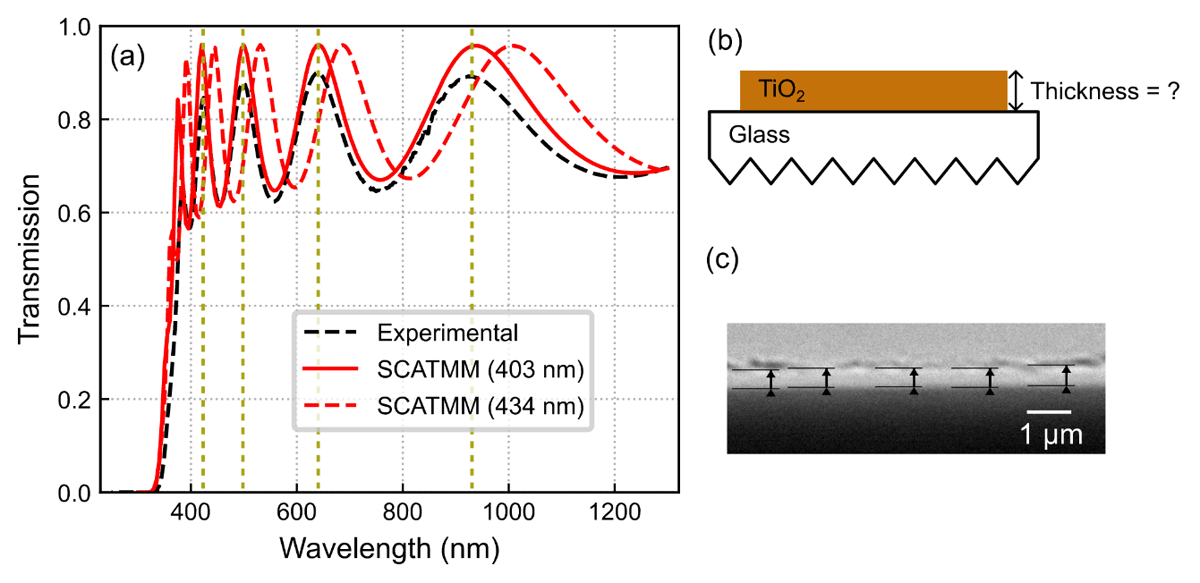
Figure 8
(a) Comparison between the spectra of the experimental measured transmission via spectrophotometry (black dashed lines) and the SCATMM transmission for both the best peak-matching thickness of 403 nm (full red line), and a thickness equal to the average profilometry measurement of 434 nm (dashed red line). (b) Schematic of the SCATMM simulation configuration, namely the TiO2 top layer and the glass substrate. The corrugated glass bottom indicates that it was defined as an infinite layer. (c) Cross-sectional SEM image of the TiO2 layer. The arrows indicate the different places measured to determine the average thickness.
As a simple illustrative example, we determined the thickness of a TiO2 layer — deposited via radio-frequency (RF) sputtering — atop of a glass substrate via peak matching of the experimentally measured transmission profile. Figure 8 (b) shows the schematic for the simulated setup, simply composed of the TiO2 film and the glass substrate taken as the bottom medium. As aforementioned, due to the relatively large substrate thickness it is approximated by an infinite medium of constant refractive index n = 1.5. Figure 8 (c) shows a scanning electron microscopy (SEM) image of the deposited layer. The measurement arrows in the figure indicate the different places where the thickness was measured, yielding a result of 437 ± 13 nm. Profilometry measurements were also taken of the sample, yielding a measured value of 434 ± 8 nm.
Figure 8 (a) presents the transmission spectra for the experimental (black dashed lines) and simulated results considering both the best (peak-matching) thickness determined with SCATMM (full red line) and the thickness of the profilometry measurement (dashed red line). For sake of simplicity, the SEM thickness was not included, as the result is close to the profilometry measurement. Although the results are quite close, 403 nm thickness determined for the SCATMM fitting with 1.8 root mean square error, against 434–437 nm (profilometry and SEM results), there is a small (<8%) disparity which is common to encounter in practical scenarios due to several reasons. One aspect concerns the slight differences in the used optical properties (refractive index spectra) of the constituent materials (here TiO2 and glass) and the actual properties of the real materials. Beyond that, the use of an infinite non-absorbent substrate medium neglects the minimal absorption of glass. This is most notable on the height difference between the transmission peaks. Another effect, and the most likely chief reason for the difference, is that it is not possible for experimentally deposited layers to have a perfectly uniform thickness across the entire area measured by spectrophotometry. While SEM and profilometry data evaluated a small region of the sample (few nm to a few μm), the transmission/reflection characterized a much larger area and thus provides a better view of the average thickness of the deposited film, while the SEM and profilometry measurements provide local measurements of the thickness. In view of that, often the SCATMM results can provide a more correct assessment of the average thickness(es) of the film(s) than local experimental measurements.
Experimental Methodology
Sample Preparation
Glass samples were cut with 2.5 × 2.5 cm2 and cleaned in 15 min of ultrasonication in isopropyl alcohol, followed by water and ethanol rinsing, and drying under a nitrogen flow.
The TiO2 film was then deposited on the glass substrates via radio frequency magnetron sputtering (see Table 1) for the duration of 120 minutes.
Optical Assessment
A UV–Vis-NIR spectrophotometer (PERKIN ELMER Lambda 950) was used to acquire the total (Tt) transmittance in the 300–1300 nm wavelength range of the TiO2 coated glass samples.
Layer Thickness Measurement
The deposited TiO2 thickness on the glass samples was determined by profilometry using a Dektak 3 Profilometer.
The thickness of the deposited layer was also analysed by cross-sectional views with a Hitachi TM 3030Plus Tabletop scanning electron microscopy (SEM) equipment. To avoid charging effects and improve the image quality in the SEM acquisition, the TiO2 film was supported on a conventional c-Si double-side polished wafer with 2 in. diameter.
Availability
Operating system
Easy-Installation:
Windows 10, 11
Manual Installation (directly run python code):
Linux (requires python with the dependencies bellow installed)
MacOs (requires python with the dependencies bellow installed)
Programming language
Python, C++, NSIS
Additional system requirements
Dependencies
Python Dependencies: python (>3.8.12), pandas (>1.3.5), numpy (>1.2), scipy (>1.7.3), matplotlib (>3.5), pyqt (>5.9.2), appdirs (>1.4.4), cython
List of contributors
Miguel Alexandre
Software location
Code repository Github
Name: The name of the code repository
Identifier: https://github.com/perspe/Scatmm
Licence: LGPL v3
Date published: 04/03/2024
Language
English
Reuse potential
This software was purpose build for simulations of solar cells, although it can be used in many other applications in the field of optics. For instance, any spectroscopic measurements of planar samples can be simulated here to compare/determine the thickness of individual layers (similar to the process shown in Section 7a.). Other examples are the determination of reflection through complex layer stacks (Bragg mirrors) and angular/polarization analysis of planar layers. Beyond that, the applications also extend to educational purposes to show optical interference — such as anti-reflection coatings — and absorption effects.
The software itself can still be improved, either by expanding the model to the simulation of non-isotropic materials (thus expanding the applicability to areas such as liquid crystals/birefringence), or by improving the interface to facilitate simulation of highly complex and specific systems, such as repeating stacks of materials or adding layer mixing via the Bruggerman (or equivalent) methods.
All modifications are welcome and can be considered to further improve the quality of the work. Furthermore, modifications can either be suggested/implemented to the lead author via email or by creating the appropriate pull request/issue in the Github page (https://github.com/perspe/Scatmm) of the project.
Notes
Funding Information
This work received funding from the FCT (Fundação para a Ciência e Tecnologia, I.P.) under the projects LA/P/0037/2020, UIDP/50025/2020 and UIDB/50025/2020 of the Associate Laboratory Institute of Nanostructures, Nanomodelling and Nanofabrication—i3N, and by the projects SpaceFlex (2022.01610.PTDC) and CO2RED (PTDC/EQU-EPQ/2195/2021), as well as by the project M-ECO2 (Industrial cluster for advanced biofuel production, Ref. C644930471-00000041) co-financed by PRR – Recovery and Resilience Plan of the European Union (Next Generation EU). The work was also supported by the European project SYNERGY (H2020-WIDESPREAD-2020-5, CSA, Grant No. 952169).
M. Alexandre and I. M. Santos also acknowledges funding by FCT, I.P. through the grants SFRH/BD/148078/2019 and 2023.03929.BD, respectively.
Competing Interests
The authors have no competing interests to declare.
Author contributions
MA developed the entire sotware package, formulated the methodology, obtained and validadated the results and wrote the main manuscript draft. IMS validated the software, obtained the experimental results and proofread the manuscript. RM provided the funding and proofread the manuscript. MJM validated the software, provided funding and proofread the manuscript.