
1. Introduction
Dicke states [1] are permutation-invariant superpositions of qubit computational basis states, for example,
These states play a prominent role in quantum information science, see e.g. the recent review [2]. Considerable effort has been devoted recently to the preparation of these states on a qubit quantum computer, see e.g., [3–9].
Considerable attention has also been devoted recently to extending qubit-based quantum computing to higher dimensions, both theoretically [10] and experimentally [11–18]. It is therefore natural to consider higher-dimensional (qudit) generalizations of Dicke states. Two such generalizations are SU(2) spin-s Dicke states and SU(d) Dicke states. An example of the former with s = 1 (and therefore 2s + 1 = 3 levels) is
with a fixed digit sum (here, 2) in each basis state. An example of the latter with d = 3 iswith one 0, one 1, and one 2 in each basis state. More precise definitions and explanations of notation can be found at the beginning of Sections 2 and 3, respectively. Potential applications of such states include quantum error correction [19,20], metrology [21], and quantum interferometric imaging [9].
Much less effort has been devoted to the preparation of qudit Dicke states than to ordinary (qubit) Dicke states. For SU(2) spin-s Dicke states, a recursive state-preparation algorithm, generalizing the one by Bärtschi and Eidenbenz [3] for qubit (s = 1/2) Dicke states, was formulated in [22]. For SU(d) Dicke states, a recursive state-preparation algorithm was formulated in [23]; and an algorithm using sorting networks has recently been formulated by Liu, Childs and Gottesman [9].
Here we consider further the problem of preparing both types of generalized Dicke states on a qudit quantum computer. We formulate quantum circuits implementing the sequential deterministic preparation [24] of these states based on their recently-found exact matrix product state (MPS) representations [25]. We also formulate circuits based on quantum phase estimation (QPE) [26,27] that prepare these states probabilistically, some of which achieve constant circuit depth, generalizing an approach developed in [4,7] for preparing ordinary Dicke states. For simplicity, we restrict our attention to exact state preparation; computational resources can be reduced by dropping this requirement [7].
The remainder of this paper is organized as follows. In Section 2, we consider the preparation of SU(2) spin-s Dicke states, starting with the sequential preparation, and then continuing with the QPE preparation. In Section 3, we consider the preparation of SU(d) Dicke states, again starting with the sequential preparation, and continuing with the QPE preparation. We briefly discuss these results Section 4. Implementations in cirq [28] of all the circuits are available on GitHub [29].
A summary of our main results, and a comparison with previous work, are presented in Table 1.
Table 1.
Summary of our results and comparison with previous work. Note that we report here worst-case values, corresponding to k ∼ sn and for and , respectively; see the respective sections for more comprehensive discussions.
| Dicke state | Reference | Depth | Ancillas [Dimension] | Repetitions |
|---|---|---|---|---|
| SU(2) spin-s | NRR [22] | 𝒪(skn) | 0 | 1 |
| Result 1 | 𝒪(skn) | 1 [k + 1] | 1 | |
| Result 2 | 𝒪 (log(sn)) | 𝒪(log(sn) + n) [2] | ||
| Result 3 | 𝒪(1) | 𝒪(n) [2sn + 1] | ||
| Result 4 | 𝒪(1) | 𝒪(log(sn)) [2], 𝒪(n log(sn)) [2s + 1] | ||
| SU(d) | NR [23] | 𝒪(nd) | 0 | 1 |
| LCG [9] | 𝒪(log n) | 𝒪(n log n + log d) [2] | 𝒪(1) | |
| Result 5 | 𝒪((n/d)d) | 1 [2], 1[𝒪((n/d)d)] | 1 | |
| Result 6 | 𝒪(d log n) | 𝒪(d log n + n) [2] | 𝒪(n(d−1)/2) | |
| Result 7 | 𝒪(d) | 𝒪(n + d) [n + 1] | 𝒪(n(d−1)/2) | |
| Result 8 | 𝒪(1) | 𝒪(d log n) [2], 𝒪(nd log n) [d] | 𝒪(n(d−1)/2) |
2. SU(2) Spin-s Dicke States
The ordinary qubit Dicke state can be written as , where is the total spin-lowering operator for a system of n spin-1/2 spins (qubits), which is applied k times on the product state . A natural higher-dimensional generalization is to consider instead spin-s spins (that is, (2s + 1)-level qudits, where s = 1/2, 1, 3/2,…), and define the normalized state , where is now the total spin-lowering operator for a system of n such spin-s spins. An example with s = 1, n = 3 and k = 2 is given in (2), where are the standard computational basis states in the (2s + 1)-dimensional complex vector space , and tensor products are understood e.g., . Note that the digit sum in each basis state in (2) is k = 2.
Spin-s Dicke states have the closed-form expression [22]
where is the binomial coefficient. These states are U(1) eigenstates for any allowed value of s where 𝕂 is a Hermitian operator defined byHence, , where is the z-component of the total spin . These states also have the “duality” (charge conjugation) property [22]
which maps k ↦ 2sn – k.A recursive deterministic approach for preparing spin-s Dicke states was presented in [22]. In this section we present several additional methods of preparing these states: a sequential deterministic approach in Section 2.1, and a probabilistic approach based on QPE in Section 2.2.
2.1. Sequential Preparation
An exact canonical MPS representation for with minimal bond dimension χ = k + 1 is given by [25]
where as in (4); moreover, are basis states of an ancilla qudit of dimension χ (an underline is used here to distinguish χ-dimensional vectors from (2s + 1)-dimensional vectors), and are (k + 1) × (k + 1) matrices with elements (for 0 < k < sn)Note that if k – j > 2s(n – i + 1), and that the binomial coefficient is defined to be zero if .
The fact that the MPS is canonical implies [24] that we can define a two-qudit unitary operator Ui acting on an ancilla qudit and a “system” qudit at site i (where i = 1, 2,…, n) that performs the mapping
where the second equality follows from (9). In view of the first equality in (10) and (8), the state can be prepared sequentially as followsIn order to implement the sequential preparation (11), it is necessary to explicitly implement the unitary Ui (10), whose coefficients depend on the state of the ancilla qudit. To this end, we decompose Ui into an ordered product of simpler operators
where the product goes from right to left with increasing l, such thatThe latter condition (14) ensures that these gates do not interfere
Although a priori all operators from l = 0 to l = k could contribute to Ui, one can check that only those operators in (12) can act non-trivially.
The operators can be implemented by the quantum circuit whose circuit diagram is shown in Figure 1. The top wire is a “system” qudit of dimension 2s + 1, and the bottom wire is the MPS ancilla qudit of dimension χ = k + 1. The circle  denotes a control on the value i. The 1-qudit gate Xd and the 2-qudit controlled gate SUMd (also known as a fan-out gate) are defined as (see e.g., [10]; we remark that 1-qudit and 2-qudit gates are already becoming experimentally feasible, see e.g., [11–18])
 to denote the control of the SUMd gate, since the control qudit can have any value.) The rotation gate is defined as
where θm is given by
to denote the control of the SUMd gate, since the control qudit can have any value.) The rotation gate is defined as
where θm is given by

Figure 1.
Each rotation gate is controlled by the ancilla value l + 1, and all operations are assumed to be modulo χ. It is straightforward to check that this circuit satisfies the properties (13), (14). For , this circuit reduces to the one presented in the appendix of [25].
The complete circuit diagram for preparing the state sequentially (11) is shown in Figure 2. We therefore have the following:
Result 1.
The state can be prepared deterministically with approximate depth 𝒪(skn) for k ∼ sn, using one ancilla of dimension k + 1.
This circuit depth is comparable to that of the circuit in [22]. For k ≪ sn, the depth is lower due to the restriction on the l-values in the product (12).
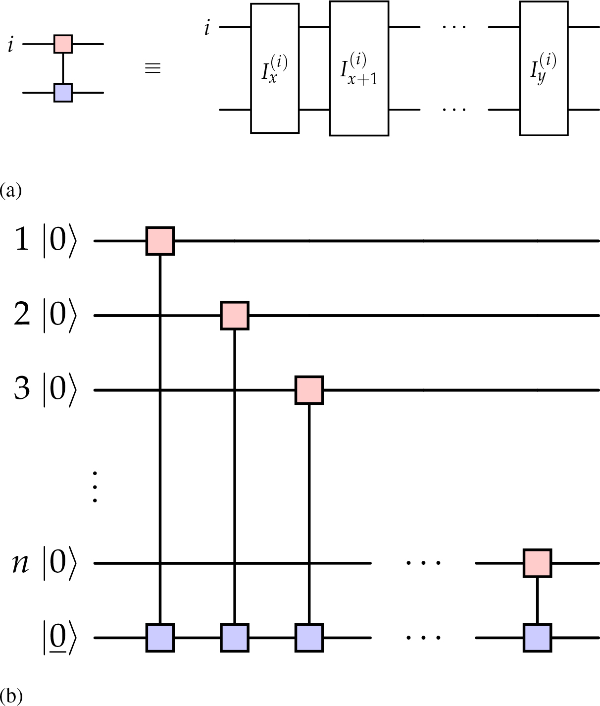
Figure 2.
Circuit diagram for preparing the state sequentially (11) (a) , with x = max(0, 2s(i – n – 1) + k) and y = min(2si – 1, k – 1); (b) .
2.2. QPE Preparation
We have seen in Section 2.1 that the sequential preparation of Dicke states is deterministic, at the cost of circuit depth that grows linearly with n. We consider here an alternative preparation method that has lower depth, but which is probabilistic. This approach is based on the quantum phase estimation algorithm [26,27], which was used in [4,7] for preparing qubit (s = 1/2) Dicke states.
The two key steps in this approach are:
constructing a suitable product state that can be expressed as a linear combination of Dicke states ; and
exploiting the U(1) symmetry of these states (5) to select the desired one.
For the first step, we observe that an n-fold tensor product of the 1-qudit state
can be expressed as the following linear combination of Dicke statesIndeed, from the definition (20), it follows that
where the last line follows from the identity (4).Borrowing a trick from [7], let us now introduce into the 1-qudit state (20) a variational parameter 0 < p < 1, which we will tune to boost the probability of preparing a Dicke state with a target value of k, see (30) below. Hence, we instead make use of the 1-qudit state
which can be similarly shown to satisfyThe state |ψ(s, p)〉 (23) can be prepared using a product of rotation gates (18) as follows
with the rotation anglesFor the second step, we define the n-qudit unitary operator
where 𝕂 and are defined in (6), and ℓ is still to be determined (see (32) below). The Dicke state is an eigenstate of this operator by virtue of (5). The QPE circuit (discussed in Section 2.2.1 below) uses the unitary operator (27) to project the product state (24) to the Dicke state with a probability P(k) given by which is maximized forThe success probability of preparing is therefore given by
where we have used Stirling's approximation. In the worst case k = sn, the number of required repetitions is . For k ≪ sn, fewer repetitions are needed, since then .2.2.1. Log Depth
The circuit diagram for the standard QPE algorithm is shown in Figure 3. The bottom wire represents the n-qudit product state (24). There are ℓ qubit ancillas, where ℓ is the minimum number of bits ki ∈ {0, 1} required to represent the maximum possible value of , namely,
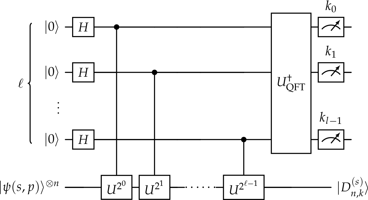
Figure 3.
Circuit diagram for preparing the state in log depth using the standard QPE algorithm. All ancilla wires are qubits. The initial state of the bottom wire is (24), and U is defined in (27).
The controlled unitaries are controlled versions of the unitary operator (27). The state of the system just prior to the measurement is
where P(k) is given by (31). The circuit therefore succeeds on measuring the ancilla qubits’ base-10 value to be the k of choice.The circuit has ℓ controlled unitaries, each of which can be implemented in constant depth using mid-circuit measurement/feedforward and n additional qubit ancillas, see Result 1 in [7]. Hence, the controlled unitaries can be implemented in depth 𝒪(ℓ). The inverse quantum Fourier transform can also can be implemented in depth 𝒪(ℓ). We therefore have the following:
2.2.2. Constant Depth
Variations of the above circuit can prepare the state in constant depth, at the expense of introducing additional and/or higher-dimensional ancillas.
The simplest such scheme, shown in Figure 4, uses the Hadamard test with an auxiliary qudit (top wire) of dimension d = 2sn + 1, which is the number of possible values k-values. The gate Hd is the generalized Hadamard gate (see e.g., [10])
and the controlled-𝒰 gate is defined as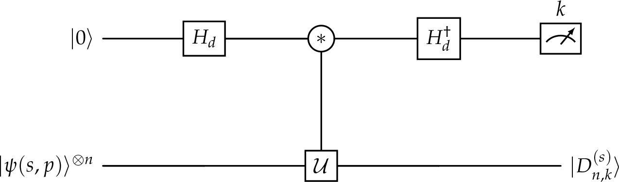
Figure 4.
Circuit diagram for preparing the state in constant depth using the Hadamard test. The top wire is a qudit of dimension d = 2sn + 1. The initial state of the bottom wire is (24), and 𝒰 is defined in (35).
This gate can be implemented in constant depth using mid-circuit measurement/feedforward and n additional ancilla qudits of dimension d, by a generalization of the proof of Result 1 in [7], see also appendix A in [30]. We therefore have the following:
Result 3.
The state can be prepared probabilistically with at worst repetitions and with depth 𝒪(1), using 𝒪(n) ancillas of dimension 2sn + 1.
The scaling of an ancilla dimension with n is an evident shortcoming of this approach.
An alternative scheme, adapted from [7], only requires ancillas of dimensions 2 and 2s + 1. The initial state (24) can be written, with the help of the identity (4), as
where S(n, s, k′) is the set of all permutations w = mn … m2 m1 of n integers, each of which is between 0 and 2s, and which sum to k′; and |w〉 = |mn … m2 m1〉 is the computational basis state of n qudits corresponding to the permutation w. We fan out ℓ – 1 times the state |w〉 (using n(ℓ – 1) ancilla qudits of dimension 2s + 1, and corresponding qudit fan-out gates) to obtain the stateAs shown in Figure 5, using ℓ qubit ancillas as controls, we then apply a product of controlled gates V defined by
where 𝕂 is the n-qudit operator defined in (6), and k is the k-value of the target state . The states |w〉 are eigenstates of U(x) for any w ∈ S(n, s, k′),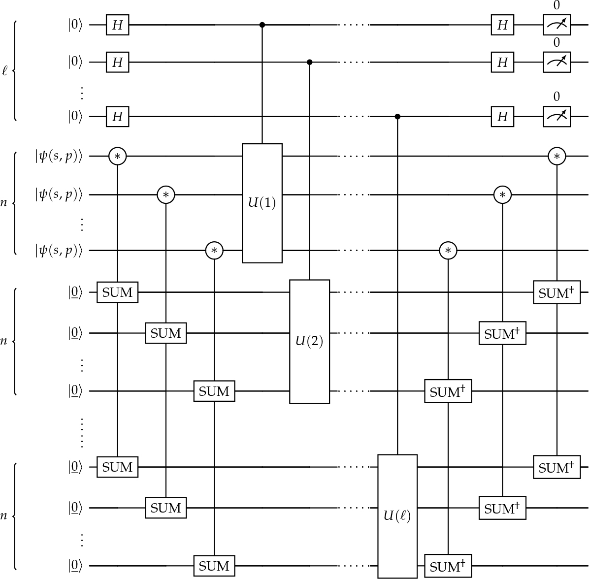
Figure 5.
Circuit diagram for preparing the state , which can be implemented in constant depth. The top ℓ wires are qubits, while all other wires are qudits of dimension 2s + 1. The state |ψ(s, p)〉 is given by (23), and U(x) is defined in (38).
With the help of the identity (for integer values of k and k′)
one can see that the state of the system just prior to measurement isThe circuit therefore succeeds on measuring all ℓ qubit ancillas to be zero.
The qudit fan-out gates (represented in Figure 5 by SUM gates) can be implemented in constant depth (see appendix A in [30]), and likewise for the V(x) gates (see Result 1 in [7]). We therefore have the following:
3. SU(d) Dicke States
Just as ordinary SU(2) Dicke states are specified by a fixed number k of |1〉’s (and therefore n – k |0〉’s), SU(d) Dicke states are characterized by a fixed vector of occupation numbers for each of d levels – that is, a specified number of d-level qudits occupying each level. Given , an SU(d) Dicke state is constructed as a uniform superposition over all computational basis states that match the specified occupation numbers.
More explicitly, let be a vector of d integers, each of which is between 0 and n, and which sum to n (that is, , and ). The corresponding n-qudit SU(d) Dicke state is defined by
where is the set of all permutations of the multiset such that ki is the multiplicity of i in , and the cardinality of is n; and |w〉 is the computational basis state of n qudits corresponding to the permutation w. Furthermore, denotes the multinomialAn example with , so that d = 3 (qutrits) and n = 3, is given by (3).
Approaches for preparing SU(d) Dicke states were presented in [9,23]. In this section we present several additional methods of preparing these states: a sequential deterministic approach in Section 3.1, and a probabilistic approach based on QPE in Section 3.2.
3.1. Sequential Preparation
An exact canonical MPS representation for was derived in [25]. The basis for the MPS ancilla consists of level sets defined by
The elements are labeled (indexed) by consecutive integers , where is the cardinality of . Here we order each level set in reverse lexicographic order, which is central for our construction, see Appendix A. Hence, for , we assign their labels such that
where lexicographic order compares vectors from left to right. Thus, if xj > yj for the first j where xj ≠ yj.For example, for so that d = 3, the level set is given by
where is a d-dimensional unit vector in the m-th direction; that is, it has components , with m = 0, 1, …, d – 1. The elements of are ordered in (47) in reverse lexicographic order, and have labels for m = 0, 1, 2.A canonical MPS with minimum bond dimension is given by [25]
where are χ × χ matrices with elements where and . The coefficient is zero unless .The fact that the MPS is canonical implies [24] that we can define a two-qudit unitary operator Ui acting on an ancilla qudit (for ) and a “system” qudit at site i ∈ {1, 2,…, n} that performs the mapping
It follows that the state can be prepared sequentially as follows
In order to formulate a circuit implementation of the sequential preparation (51), it is necessary to devise a circuit for the unitary Ui (50). Proceeding as in Section 2.1, we decompose Ui into an ordered product of simpler operators
where the product goes from right to left with increasing label , such that andThe operators can be implemented by the quantum circuit whose circuit diagram is shown in Figure 6. The top wire is a “system” qudit of dimension d, and the middle wire is the MPS ancilla qudit of dimension χ. In contrast with the corresponding SU(2) spin-s circuit in Figure 1, there is an additional (bottom) wire representing a qubit ancilla. The level sets , the corresponding labels and their inverses are computed classically.
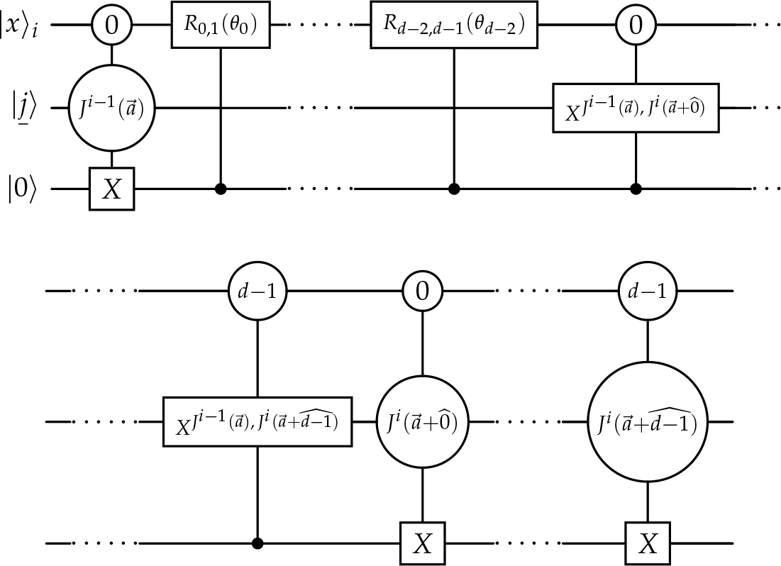
Figure 6.
Circuit diagram for .
In Figure 6, for the case that both x = 0 and , corresponding to the first condition (53), the state of the qubit ancilla is flipped to |1〉 by the double-controlled NOT; the controlled rotation gates (18) with angles
generate the coefficients in (53). After the rotations, the state of the MPS ancilla qudit is mapped to for m = 0, 1,…, d − 1 by a series of double-controlled-Xi,j gates, where the 1-qudit gate Xi,j is defined asFinally, the qubit ancilla is reset to |0〉 by a series of double-controlled NOTs.
The second condition (54) requires for . In order for the circuit in Figure 6 to satisfy this condition, it is necessary (to avoid triggering the double-controlled-NOT with the control value near the end of the circuit) that
which is guaranteed by our labeling of the level sets in reverse lexographic order. Indeed, we exploit this ordering to show in Appendix A that for all , from which (58) follows.Finally, it is straightforward to check that the third condition (55), which ensures that these gates do not interfere, is also satisfied by the circuit in Figure 6. The full circuit for the sequential preparation (51), including all Ui operators, has the same structure as in Figure 2b.
We see from (52) that each Ui is made of -many I(i)-operators; and we see from Figure 6 that each I(i)-operator is made of 3d gates. Hence, the total circuit depth is . Although a closed-form expression for is not known, it has the “stars and stripes” bound , which leads to an approximate circuit depth 𝒪((n/d)d). A similar result is obtained by considering the worst case , for which . We therefore have the following:
Result 5.
The state can be prepared deterministically with a worst-case approximate depth 𝒪((n/d)d), using one qubit ancilla, and one ancilla of dimension .
The circuit depth is significantly smaller for typical -values. For example, for of the form
or any permutation thereof, we find that χ ≤ (x + 1)r, implying an approximate depth 𝒪(xrn).3.2. QPE Preparation
We now consider a probabilistic approach of preparing the Dicke states that is based on the quantum phase estimation algorithm [26,27]. As in the case of SU(2) spin-s Dicke states discussed in Section 2.2, there are two key steps:
constructing a suitable product state that can be expressed as a linear combination of Dicke states ; and
exploiting the U(1)⊗(d−1) symmetry of these states (see (68) below) to select the desired one.
For the first step, we observe that the n-fold tensor product of the 1-qudit state
can be expressed as the following linear combination of Dicke statesIndeed,
In passing to the second line of (63), we used the fact
where the multiset is defined in (43); and the third line of (63) follows from the definition (42) of the Dicke state .To boost the probability of preparing a Dicke state with a target -value, we introduce d variational parameters 0 < ξi < 1 into the 1-qudit state (61)
which can be similarly shown to satisfyThe 1-qudit state (65) can be prepared using a product of rotation gates similarly to (25).
For the second step, we define the d – 1 Hermitian and mutually-commuting operators 𝕂(1), …, 𝕂(d–1) as follows
The Dicke states are simultaneous eigenstates of all these operators
We define the corresponding unitary operators
where ℓ is still to be determined (see (74) below), of which the Dicke states are simultaneous eigenstatesThe QPE circuit (discussed in Section 3.2.1 below) uses the unitary operators (69) to project the product state (66) to the Dicke state with a probability given by
which is maximized forThe success probability of preparing is therefore given by
In the worst case , the number of required repetitions is . For typical -values, significantly fewer repetitions are needed. For example, for the case (60), .
3.2.1. Log Depth
The circuit diagram for the standard QPE approach is shown in Figure 7. The bottom wire represents the n-qudit product state (66). There are (d – 1) ℓ qubit ancillas, where ℓ is the number of bits of n (recall that 0 ≤ ki ≤ n), namely,
The controlled unitaries are controlled versions of the unitary operators (69). The state of the system just prior to the measurement is
where is given by (73). The circuit therefore succeeds on measuring the ancilla qubits’ base-10 values to be those of the target .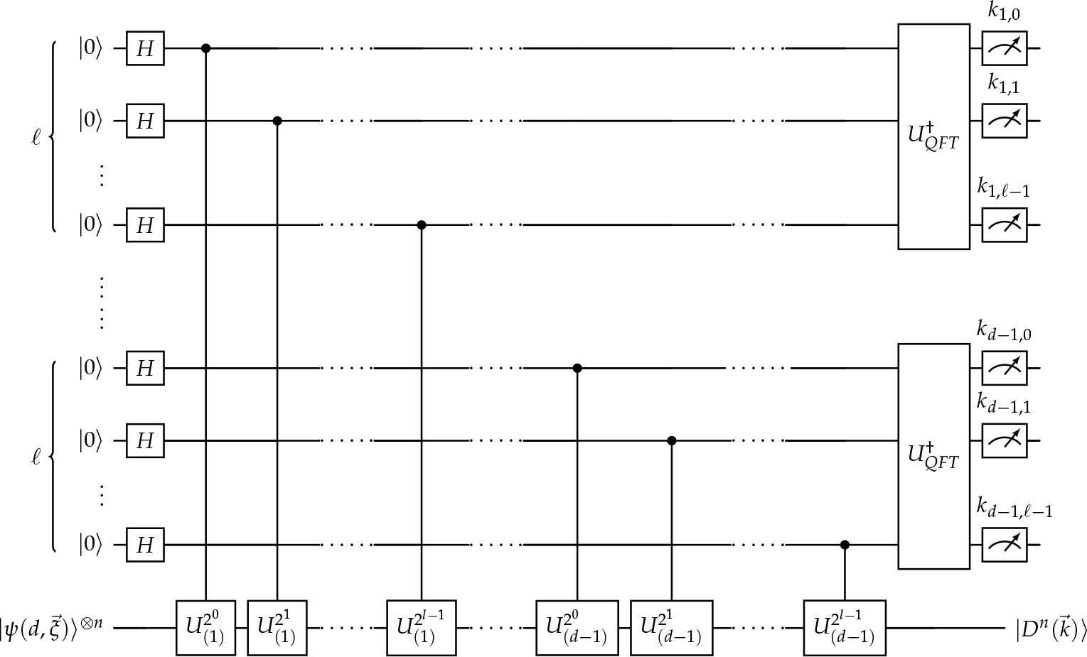
Figure 7.
Circuit diagram for preparing the state in log depth using the standard QPE algorithm. All ancilla wires are qubits. The initial state of the bottom wire is (66), and U(i) is defined in (69).
This circuit is evidently similar to the SU(2) spin-s version in Figure 3, differing mainly in the number of ancillas: the latter has only ℓ, while the former has (d – 1)ℓ in order to access all components of . Each of the (d – 1)ℓ controlled unitaries can be implemented in constant depth using measurement/feedforward and n additional qubit ancillas, see Result 1 in [7]. Hence, the controlled unitaries can be implemented in depth 𝒪((d – 1)ℓ). Each inverse quantum Fourier transform can be implemented in depth 𝒪(ℓ). We therefore have the following:
3.2.2. Constant Depth
Similarly to the case of SU(2) spin-s Dicke states discussed in Section 2.2.2, variations of the above circuit can prepare the state in constant depth, at the cost of introducing additional and/or higher-dimensional ancillas.
The circuit in Figure 8 consists of (d – 1) separate Hadamard tests using auxiliary qudits of dimension 𝔡 = n + 1, which is the number of possible values for each ki. The controlled-U(i) gates are defined, for i = 1, …, d – 1, as
where 𝕂(i) and are defined in (67). These gates can be implemented in constant depth using measurement/feedforward and n additional ancilla qudits of dimension 𝔡, by a generalization of the proof of Result 1 in [7], see also appendix A in [30]. We therefore have the following: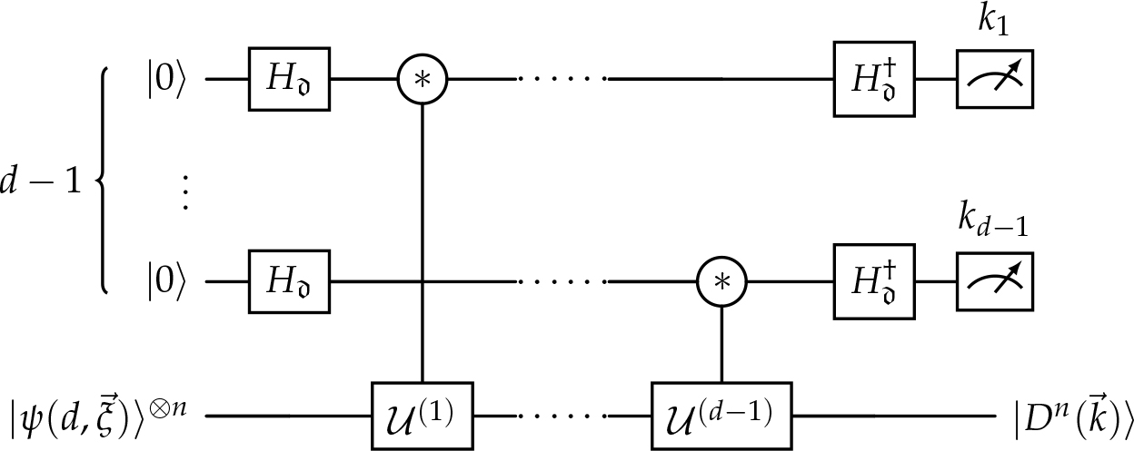
Figure 8.
Circuit diagram for preparing the state in constant depth using Hadamard tests. All ancilla wires are qudits of dimension 𝔡 = n + 1. The initial state of the bottom wire is (66), and 𝒰(i) is defined in (76).
Result 7.
The state can be prepared probabilistically with at worst 𝒪(n(d–1)/2) repetitions and with depth 𝒪(d) (independent of n), using 𝒪(n + d) ancillas of dimension n + 1.
Finally, we can formulate an alternative constant-depth SU(2) circuit using ancillas of dimensions 2 and d, by generalizing the SU(d) spin-s circuit in Figure 5. Similarly to (36), the initial product state (66) can be re-expressed as a superposition of computational basis states |w〉
where the multiset is defined in (43). We fan out (d – 2)ℓ + (ℓ – 1) = (d – 1)ℓ – 1 times the state |w〉 (using n((d – 1)ℓ – 1) qudit ancillas of dimension n, and corresponding qudit fan-out gates, denoted by F in Figure 9) to obtain the state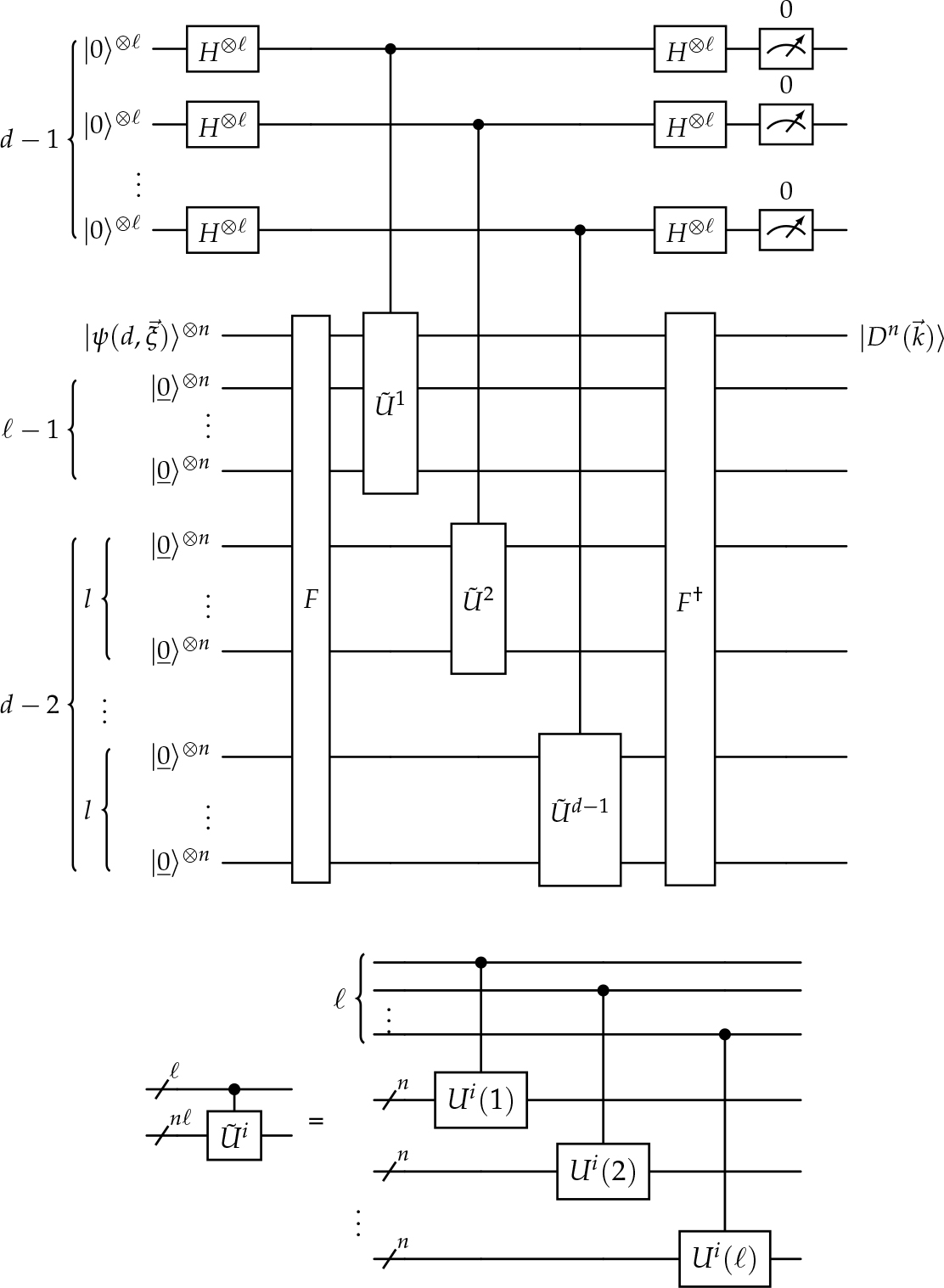
Figure 9.
(a) Circuit diagram for preparing the state in constant depth. Each of the top (d – 1) wires represent ℓ qubits, while each of the other wires represent n qudits of dimension d. F is a fan-out gate. (b) Decomposition of the sub-circuit, where Ui(x) is defined in (79).
We then use (d – 1)ℓ qubit ancillas to apply a product of controlled gates Vi defined by
where is the -value of the target state . With the help of the identity (40), one can see that the state of the system just prior to measurement isThe circuit therefore succeeds on measuring all (d – 1)ℓ qubit ancillas to be zero.
The qudit fan-out gates can be implemented in constant depth (see appendix A in [30]), and likewise for the Vi(x) gates (see Result 1 in [7]). We therefore have the following:
4. Discussion
We have presented a number of new ways of preparing qudit Dicke states. The circuits are explicit and straightforward, and are arguably simpler than those previously reported. (Implementations in cirq [28] of all the circuits are available on GitHub [29].) Indeed, for SU(2) spin-s Dicke states, the sequential preparation circuits in Section 2.1 do not require separate treatment of “edge” cases, and do not require double-controlled gates, as does the circuit in [22]; and the corresponding QPE circuits in Section 2.2 are even simpler and have lower depth, albeit at the expense of using additional and/or higher-dimensional ancillas and requiring multiple repetitions. For SU(d) Dicke states, the comparison of the results in Sections 3.1 and 3.2 with that of [23] is similar. The corresponding algorithm in [9] has a superior blend of depth, ancillas and repetitions (see Table 1), but is considerably more complicated.
For the sequential preparation circuits, it would be in interesting to see if mid-circuit measurement and feedforward (local operations and classical communication, or LOCC) could be used to reduce circuit depth, as has been achieved for the preparation of multiqubit states, see e.g., [5,7,30–34].
A feature of the circuits in [22,23] is that they can straightforwardly prepare superpositions of Dicke states, following Theorem 2 in [3]. A separate algorithm for preparing superpositions of SU(d) Dicke states is also presented in [9]. However, the circuits presented here will require modification and/or additional overhead in order to prepare such superpositions. For example, starting from the SU(2) spin-s circuit using the Hadamard test in Figure 4, one can add a qudit ancilla encoding the amplitudes of the target superposition of Dicke states (which is ultimately measured), and add suitable gates encoding the corresponding k-values; however, the success probability of preparing the target superposition will be smaller than for the original circuit, due to the measurement of the additional ancilla.
Acknowledgments
We thank David Raveh for valuable discussions and comments on a preliminary draft.
Notes
[1] Contributed by Author Contributions
R.N. (Conceptualization: Lead; Methodology: Lead; Project administration: Lead; Supervision: Lead; Formal analysis: Lead; Investigation: Equal; Writing - original draft: Equal; Writing - review and editing: Equal); N.K. (Software: Lead; Formal analysis: Supporting; Investigation: Equal; Writing - original draft: Equal; Writing - review and editing: Equal); F.G. (Software: Supporting; Investigation: Supporting). All authors have read and agreed to the published version of the manuscript.
[2] Conflicts of interest Conflicts of Interest Statement
The authors declare no conflicts of interest.
Appendices
Appendix A. Proof of Eq. (59)
We provide here a proof of Eq. (59), which is equivalent to the Proposition below. We use the notation introduced in Section 3.1. Our proof makes use of the following lemma.
Proof.
We prove the contraposition. That is, we show that the assumption leads to a contradiction of the premise. Indeed, let us suppose that
Then the zeroth component of must be zero, i.e., y0 = 0. This implies that
In other words, , which contradicts the premise.
We are now ready to prove the following proposition.
Proof.
Define . Then there exist p elements such that
and thereforeMoreover, the Lemma implies that there are no additional elements (beyond those elements in (A5)) that satisfy . We conclude that
as desired.We note that the equality holds in (A6) if for all values of r, which occurs if i + 1 ≤ k0. Indeed, in this case, (since implies that ), and therefore .
On the other hand, if i + 1 > k0, then there exists an element defined by
that has 0 index, i.e. . Hence, (since implies that a0 < k0, while ξ0 = k0) and . Referring again to (A5), we see that for at least one value of r, which leads to a strict inequality in (A6).