
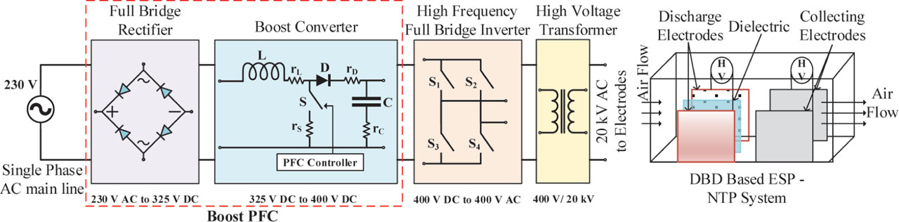
Figure 1.
Block diagram of the HV power supply system for a DBD-based ESP–NTP system. DBD, dielectric barrier discharge; ESP, electrostatic precipitators; HV: high voltage; NTP, non-thermal plasma; PFC, power factor correction.
Table 1.
Design specification for boost PFC.
| Parameters | Value | Parameters | Value |
|---|---|---|---|
| Input voltage | 230V AC | Switching frequency | 50 kHz |
| Boost output voltage | 400V DC | PFC inductor | 6.6 mH |
| Output power | 900 W | Equivalent load resistance | 177.78 Ω |
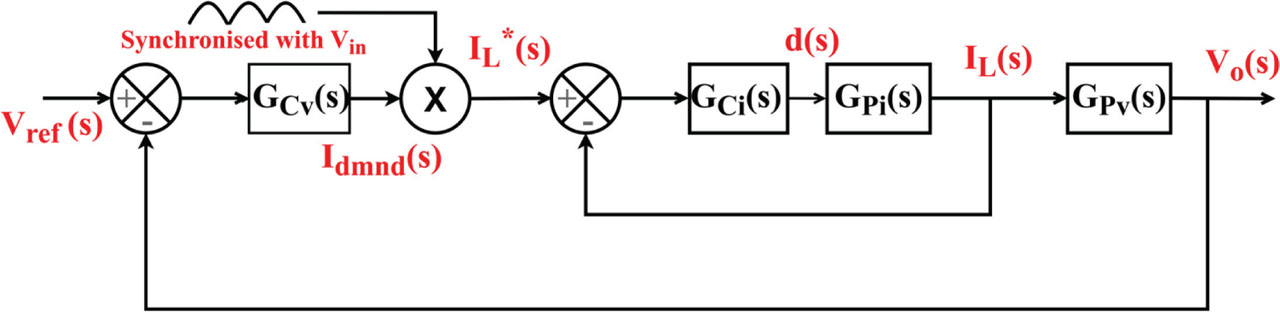
Figure 2.
PFC control block diagram. PFC, power factor correction.
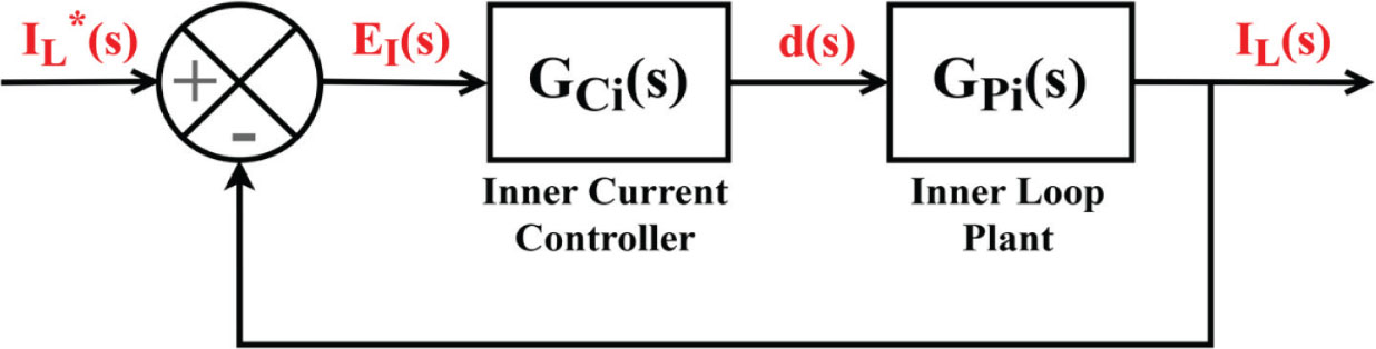
Figure 3.
Inner current control loop in boost PFC systems. PFC, power factor correction.
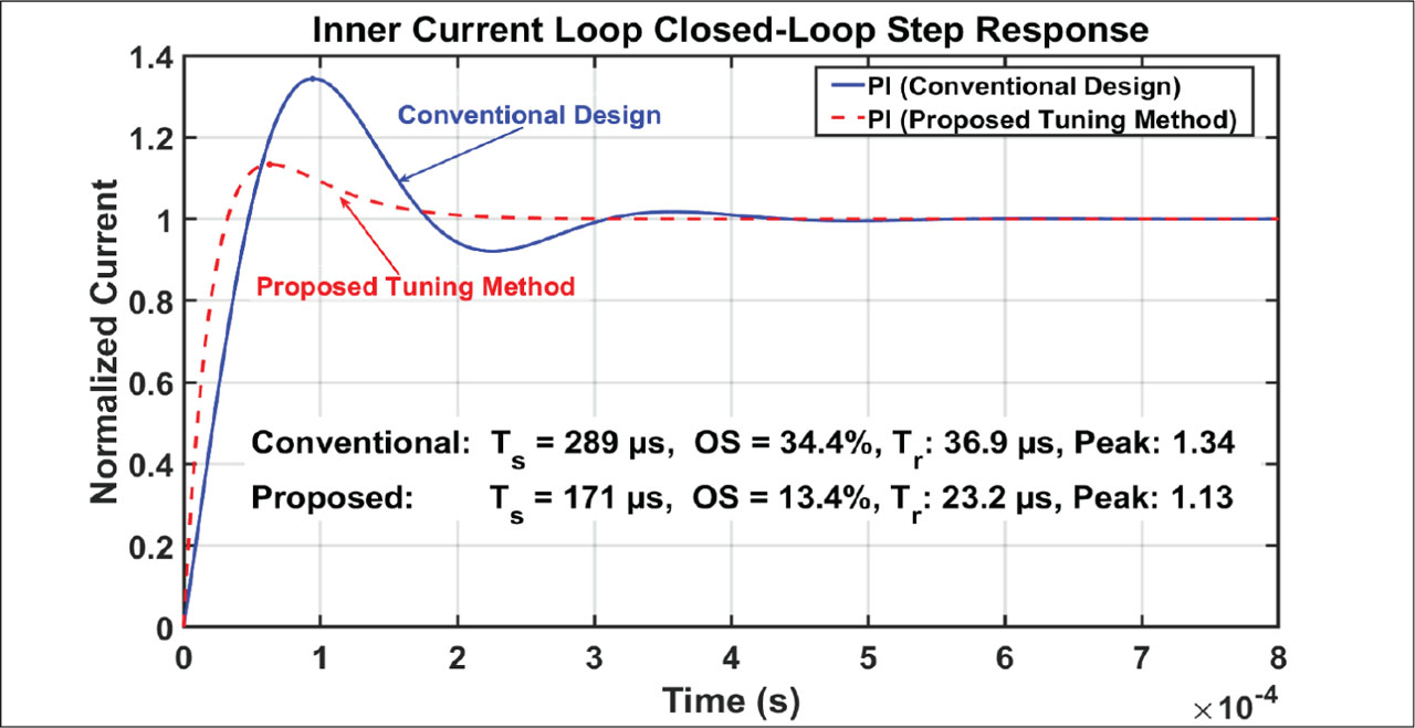
Figure 4.
Closed-loop step responses of the inner current loop with different PI tuning methods. Ts: Settling time, OS: overshoot, Tr: rise time. PI, proportional integral.
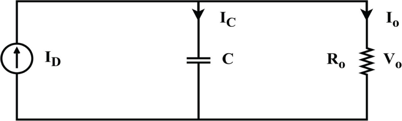
Figure 5.
Simplified equivalent circuit diagram of boost PFC based on average power. PFC, power factor correction.
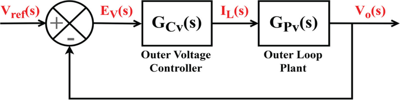
Figure 6.
Outer voltage control loop in boost PFC systems. PFC, power factor correction.
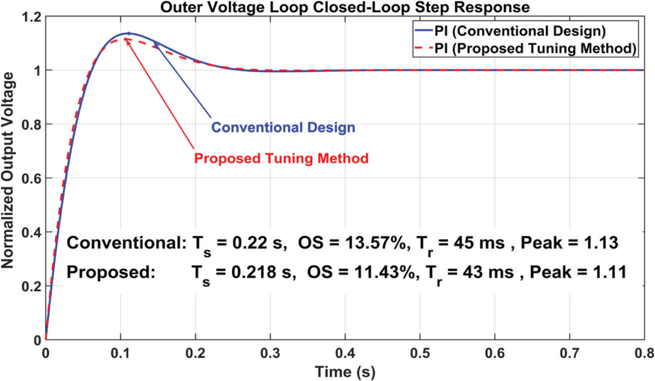
Figure 7.
Closed-loop step responses of the outer voltage loop with different PI tuning methods. Ts: Settling time, OS: overshoot, Tr: rise time. PI, proportional integral.
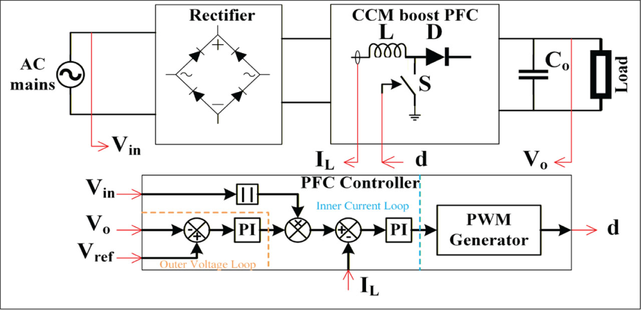
Figure 8.
Control architecture of boost PFC converter with dual-loop regulation. PFC, power factor correction; PI, proportional integral.
Table 2.
Qualitative comparative performance of inner current control strategies for boost PFC converters.
| Performance parameter | PI | PR | HCC | DB | MPC | MFPC | SMC | Proposed PI |
|---|---|---|---|---|---|---|---|---|
| Computational and implementation aspects | ||||||||
| Computational burden (per cycle) | L | M | L | H | VH | M | M | L |
| Implementation complexity | L | M | L | H | VH | M | H | L |
| Parameter sensitivity | M | M | L | VH | H | L | VL | M |
| Dynamic performance | ||||||||
| Current transient response | S | F | VF | VF | VF | F | F | S |
| Phase error (grid frequency) | NZ | Z | NrZ | Z | NrZ | NrZ | Z | NrZ |
| Steady-state performance | ||||||||
| Steady-state current THD | >5% | <5% | <3% | <5% | <2% | <5% | <3% | <5% |
| Steady-state error | NZ | Z | NrZ | Z | NrZ | NrZ | Z | NrZ |
[i] DB, deadbeat; F, fast; H, high; HCC, hysteresis current control; L, low; M, moderate; MFPC, model-free predictive control; MPC, model predictive control; NrZ, near zero; NZ, non-zero; PI, proportional integral; PR, proportional resonant; S, slow; SMC, sliding mode control; VF, very fast; VH, very high; Z, zero.
Table 3.
Experimental hardware specifications and statistical performance parameters of the compared control strategies.
| Control strategy (references) | Rated power (W) | Vin/Vout (V) | Output capacitor (μF) | Switching frequency (kHz) | THD (%) | PF |
|---|---|---|---|---|---|---|
| PI: Okilly and Baek (2022) | 2,000 | 220/400 | 950 | 100 | 5.5 | 0.9935 |
| PR: Liu et al. (2013) | 3,000 | 220/400 | 940 | 19.2 | N.R | N.R |
| HCC: Shehata et al. (2023) | 100 | 40/100 | 1,000 | 21 | 2.61 | 0.999 |
| DB: Mattavelli et al. (2005) | 400 | 230/400 | 330 | 50 | N.R | N.R |
| MPC: Israr and Samuel (2025) | 500 | 220/400 | 100 | 20 | 1.8 | 0.999 |
| MFPC: Gu et al. (2021) | 1,000 | 110/300 | 990 | 50 | N.R | 0.99 |
| SMC: Mohanty and Panda (2016) | 500 | 230/390 | 470 | 200 | 2.4 | 0.999 |
| Proposed work (FDM-GART PI) | 900 | 230/400 | 1,000 | 50 | 4.7 | 0.999 |
[i] N.R. = Not explicitly reported in the text.DB, deadbeat; FDM, frequency-differentiated modelling; GART, grid-aligned resonance tuning; HCC, hysteresis current control; MFPC, model-free predictive control; MPC, model predictive control; PF, power factor; PI, proportional integral; PR, proportional resonant; SMC, sliding mode control; THD, total harmonic distortion.
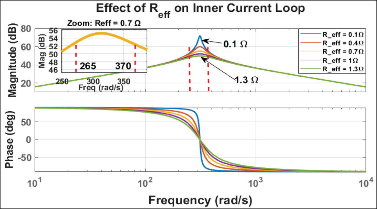
Figure 9.
Bode analysis of the effect of Reff on the inner current loop.
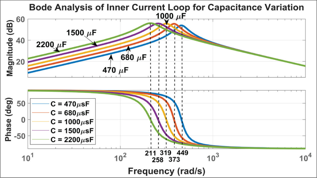
Figure 10.
Bode analysis of inner current loop for capacitor variations.
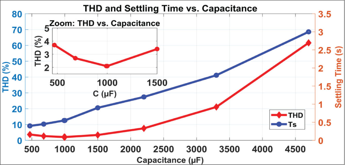
Figure 11.
Combined plot of THD and settling time versus output capacitance. THD, total harmonic distortion.
Table 4.
Simulation parameters.
| Parameters | Value | Parameters | Value |
|---|---|---|---|
| Output capacitor | 1,000 µF | Switch on-resistance | 0.25 Ω |
| ESR of capacitor | 0.1076 Ω | Forward resistance of diode | 0.03 Ω |
| Resistance of the inductor | 0.5 Ω | Diode cut-in voltage | 1.05V |
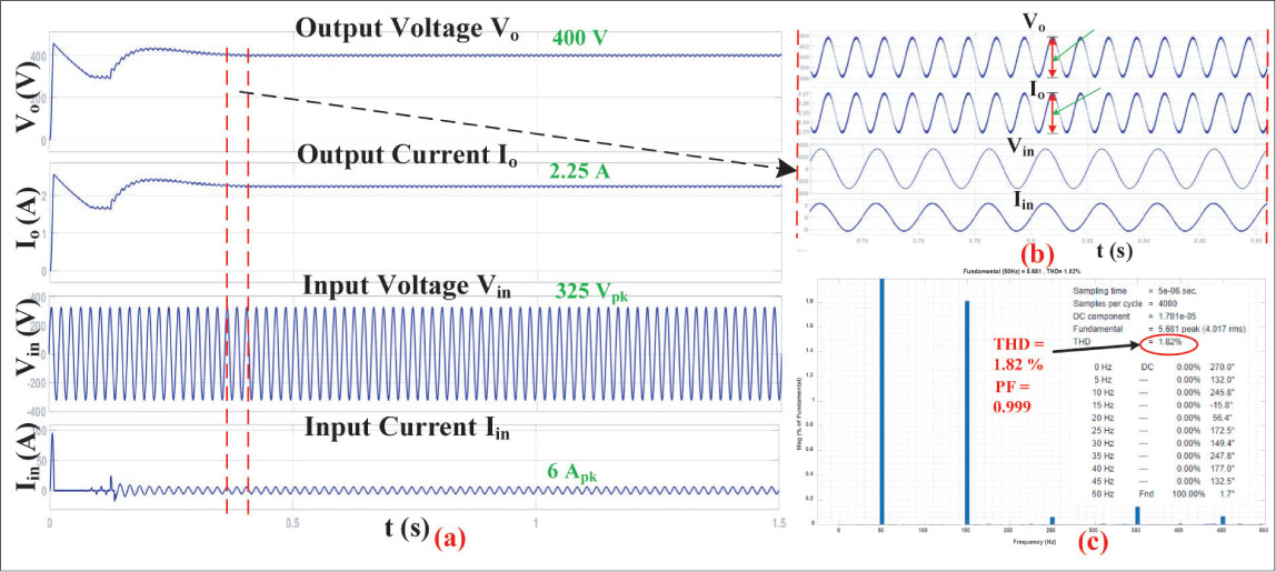
Figure 12.
(a) Steady-state operation of boost PFC under rated load conditions; (b) Zoomed-in waveform showing input current tracking input-voltage and output-voltage ripple; (c) THD of input current. PFC, power factor correction; THD, total harmonic distortion.
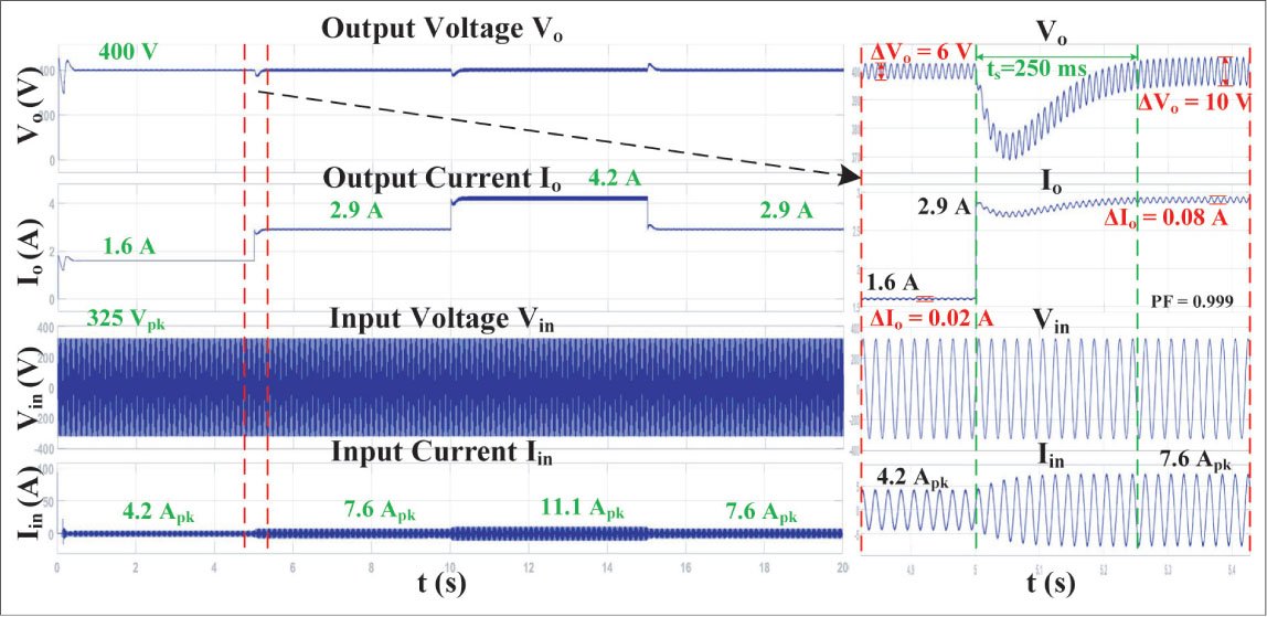
Figure 13.
Load regulation performance of boost PFC converter. PFC, power factor correction.
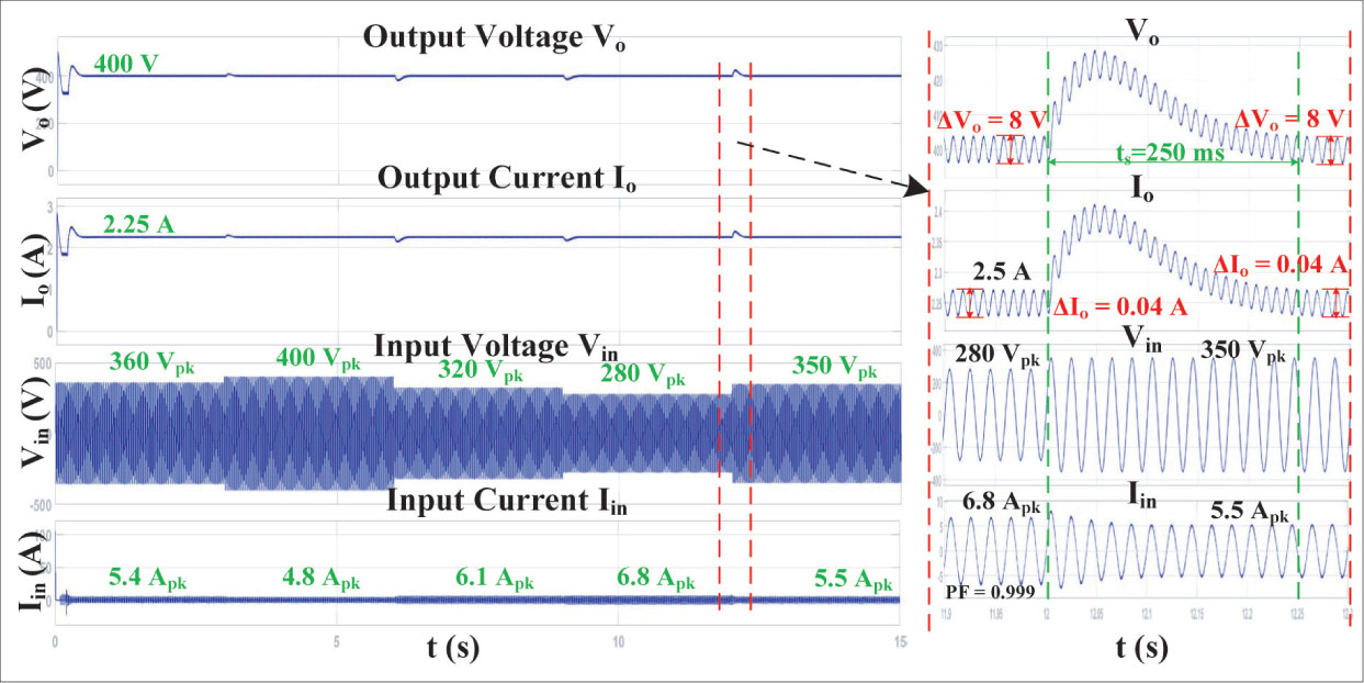
Figure 14.
Line regulation performance of boost PFC converter. PFC, power factor correction.
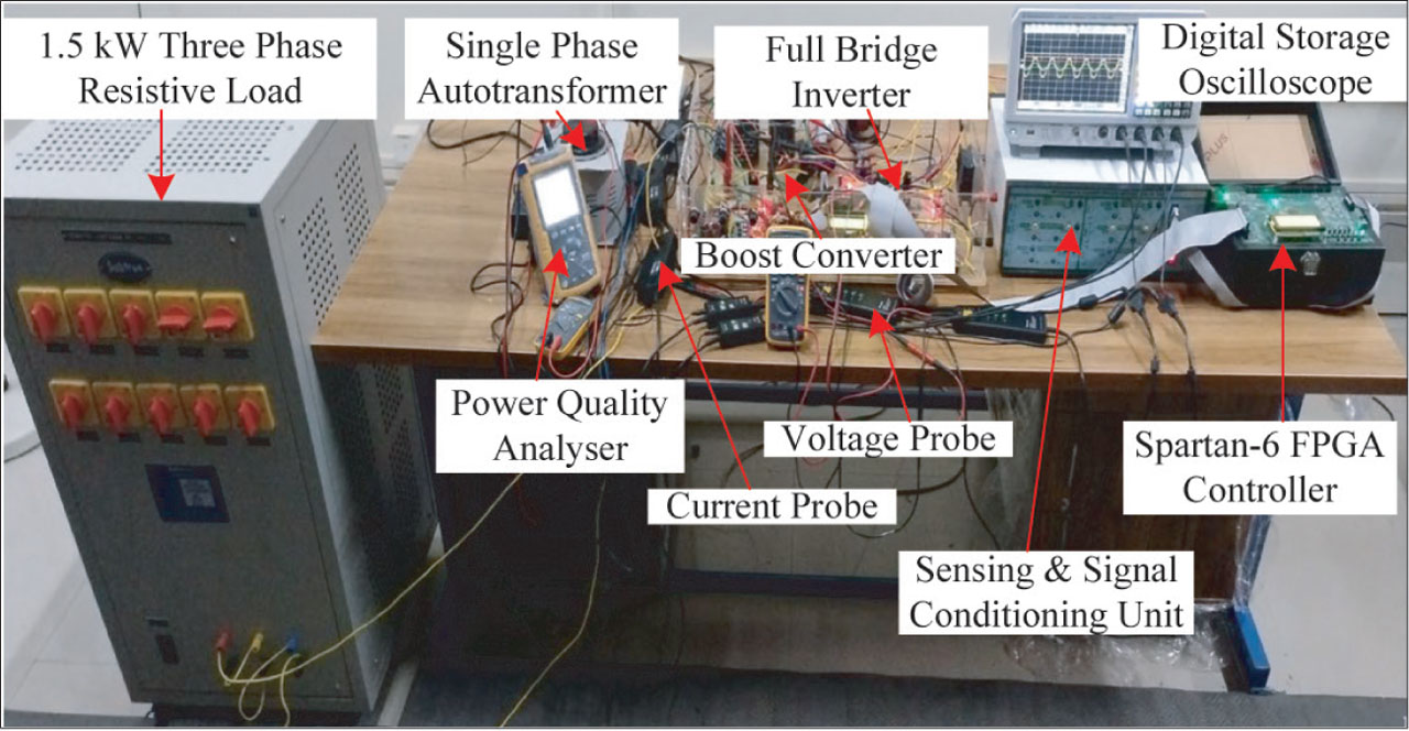
Figure 15.
Experimental hardware setup of the 900 W boost PFC prototype. PFC, power factor correction.
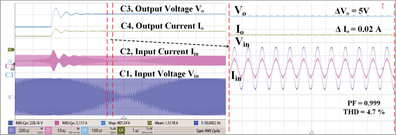
Figure 16.
Input voltage Vin (C1: 200V/div), input current Iin (C2: 10 A/div), output current Io (C4: 1 A/div), output voltage Vo (C3: 100V/div). PF, power factor; THD, total harmonic distortion.
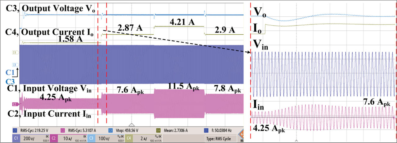
Figure 17.
Load regulation performance of boost PFC converter. Input voltage Vin (C1: 200V/div), input current Iin (C2: 10 A/div), output current Io (C4: 2 A/div), output voltage Vo (C3: 100V/div). PFC, power factor correction.
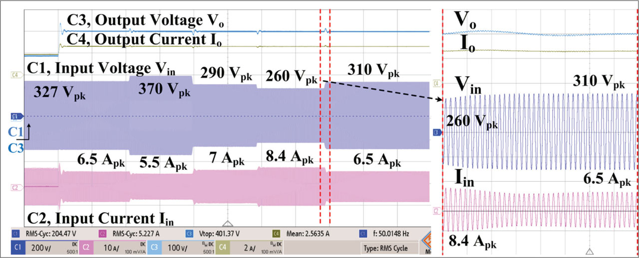
Figure 18.
Line regulation performance of boost PFC converter. Input voltage Vin (C1: 200V/div), input current Iin (C2: 10 A/div), output current Io (C4: 2 A/div), output voltage Vo (C3: 100V/div). PFC, power factor correction.
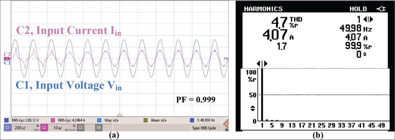
Figure 19.
(a) Input-current waveforms before and after PFC activation. (b) THD measurement. PF, power factor; PFC, power factor correction; THD, total harmonic distortion.
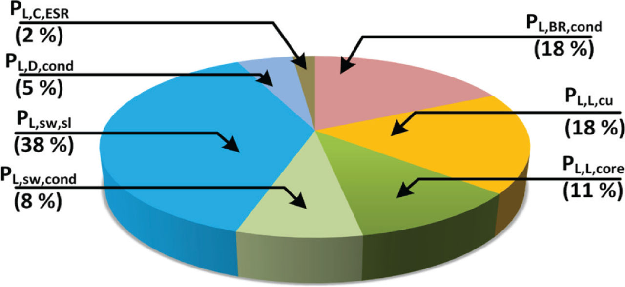
Figure 20.
Power loss distribution of the boost PFC converter. PFC, power factor correction.
Table 5.
Analytical loss models and derived current expressions for the PFC converter power-stage components.
| Components | Loss model | Analytical expression | Derived current expressions used for loss calculation |
|---|---|---|---|
| Bridge rectifier | Conduction loss, PL,BR,cond | ||
| Inductor | Copper loss, PL,L,cu | ||
| Core loss, PL,L,core | |||
| Switch (MOSFET) | Conduction loss, PL,sw,cond | ||
| Switching loss, PL,sw,sl | |||
| Diode | Conduction loss, PL,D,cond | ||
| Capacitor | ESR, PL,C,ESR |
[i] ESR, equivalent series resistance; fs, Switching frequency; IC,avg, Average capacitor current; IC,rms, RMS capacitor current; ID,avg, Average diode current; ID,rms, RMS diode current; Iin,avg, Average input current; Iin,rms, RMS input current; IL,avg, Average inductor current; IL,rms, RMS inductor current; IO, Output current; Isw,avg, Average switch current; Isw,rms, RMS switch current; PFC, power factor correction; Pv, Volumetric core loss density; rd, diode dynamic resistance; RDS(on), MOSFET’s on-resistance; RESR, ESR of capacitor; tf, Fall time; tr, Rise time; Vc, Core volume; VF, Diode forward voltage drop; Vin,pk, Peak input voltage; VO, Output voltage.
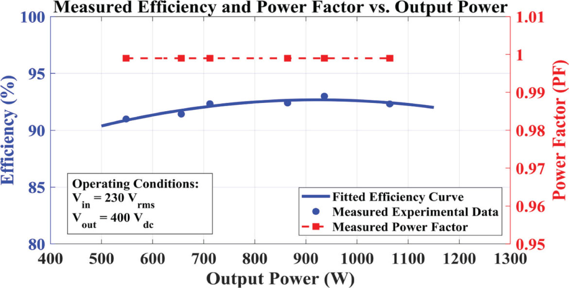
Figure 21.
Efficiency profile and PF performance of the proposed 900 W boost PFC prototype operating at a nominal input of 230Vrms. PF, power factor; PFC, power factor correction.