
1. Introduction
Indoor air pollution in enclosed spaces poses serious health risks from airborne particulate matter (PM) and pathogens, which can lead to respiratory and cardiovascular diseases (Chen et al., 2020; Kelly and Fussell, 2019; Nair et al., 2022). Although high-efficiency particulate air (HEPA) filters trap particulates, they cannot inactivate microorganisms and they create pressure drops that increase energy consumption (Mata et al., 2022; Watson et al., 2022). Non-thermal plasma (NTP)-enhanced electrostatic precipitators (ESPs) utilise electrostatic charging and plasma-generated reactive species for particle capture and disinfection. Studies show that NTP ionisers with ESPs effectively inactivate airborne pathogens (Afshari et al., 2020; Jung and Kim, 2017; Lai et al., 2016; Li et al., 2024b; Parker, 2003). Dielectric barrier discharge (DBD) is ideal for NTP–ESP air purification. Unlike industrial ESP corona discharges that produce sparks, DBD uses a current-limiting dielectric barrier (Chang, 2001; Kogelschatz, 2003; Li et al., 2020). Hence, such systems require a power supply that periodically limits or reverses the electric field to prevent charge accumulation on the dielectric surface. This interruption is essential for sustaining stable NTP and suppressing arc formation, making AC or pulsed DC the preferred excitation method over DC. The DBD structure charges particles for removal via electrostatic precipitation and generates reactive species for pathogen inactivation (Asilevi et al., 2021; Li et al., 2024a), making it suitable for compact ESP–NTP systems.
Studies have shown that the efficiencies of particle removal and pathogen inactivation depend on the amplitude and frequency of the AC supply or pulsed DC supply (Chen et al., 2022; Hernández-Díaz et al., 2021; Zhang et al., 2024). Several high-voltage (HV) power supplies have been discussed in the literature which can be used for industrial ESPs. These power supplies use fixed-frequency resonant topologies to generate DC voltages. As mentioned earlier, DC voltages are unsuitable for DBD. In addition, these power supplies use complex control schemes and high-frequency HV transformers (Grass et al., 2004; Soeiro et al., 2012; Vukosavić et al., 2015). Furthermore, existing DBD power supplies typically utilise conventional inverters, multilevel converters, complex resonant systems, or voltage multiplier circuits powered by a low-to-HV DC link (Dragonas et al., 2015; Jiang et al., 2020; Liu et al., 2019). This reveals the need for a simple, modular HV AC supply with variable voltage and frequency for the evaluation of the ESP–NTP system. This power supply typically requires a rectifier, inverter, and HV transformer cascaded to provide a HV AC output. The circuit configuration is shown in Figure 1. A power factor correction (PFC) unit is required at the front end of this power supply to comply with the IEEE 519 and IEC 61000 standards (Bhat and Agarwal, 2008; Institute of Electrical and Electronics Engineers, 2018; International Electrotechnical Commission, 2018). Among the various PFC topologies reported in the literature, the boost converter remains the most widely adopted due to its simple structure, continuous input current, and effective power quality improvement characteristics (Quiroga et al., 2025). A boost converter-based PFC circuit with dual-loop control is simple and effective for loads such as DBD-based ESP–NTP systems which do not regenerate.
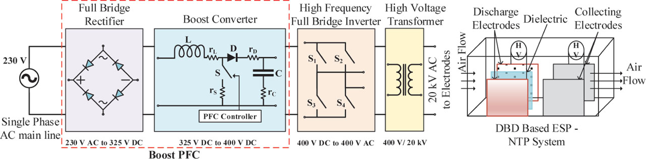
Figure 1.
Block diagram of the HV power supply system for a DBD-based ESP–NTP system. DBD, dielectric barrier discharge; ESP, electrostatic precipitators; HV: high voltage; NTP, non-thermal plasma; PFC, power factor correction.
The DBD load exhibits non-linear behaviour, acting as a capacitor before plasma inception and becoming an equivalent non-linear impedance consisting of a capacitor and non-linear resistive discharge path thereafter. As the voltage reaches the threshold, the sudden onset of discharge causes a rapid impedance shift (Kogelschatz, 2003). In poorly regulated systems, this can cause a DC bus voltage sag or current spike, leading to plasma quenching or inverter tripping. Therefore, it is essential to ensure that the DC-link capacitor provides wide-ranging decoupling between the transformer output and the DC link so that the variations in load do not affect the DC-link voltage. To ensure this, the bandwidth of the voltage control loop, which regulates the DC-link voltage, must be small. The design of the outer voltage loop in single-phase boost PFC converters is constrained by the need to suppress double-line-frequency ripple while maintaining adequate dynamic performance. Adaptive control strategies can be highly effective in suppressing DC-link ripples in boost converter applications (Wang and Zhang, 2021). Recent studies have shown that reducing DC-link capacitance further increases the importance of voltage-loop design and ripple management (Israr and Samuel, 2025). While PFC voltage loops typically operate at a 10–20 Hz bandwidth to attenuate 2 × fL output ripple (fL – line frequency), this may not sufficiently decouple the grid side current control from the DBD plasma inception impedance discontinuities. To ensure system stability while the capacitor handles the transient load demand, the outer voltage-loop bandwidth is restricted to . This wide separation between the fast-switching current dynamics and slow voltage-regulation dynamics necessitates the use of distinct models for the inner and outer loops, rather than a single time-invariant small-signal model.
The boost PFC exhibits two distinct time scales: fast-switching dynamics at fS (50 kHz) for inductor/switch behaviour and slow dynamics for rectified mains (100 Hz) and DC-link energy balance (Wong et al., 2006). Switching-averaged state space linearisation captures dynamics below but assumes a quasi-steady-state operation (Middlebrook and Ćuk, 1977). In PFC, the duty and operating point are periodically modulated by the rectified line, and the linearised coefficients become time periodic (at 2 × fL). This phenomenon is called period doubling (Wong et al., 2006). This parametric modulation creates sideband interactions and instabilities that are not captured by linear time-invariant (LTI) models (Wang et al., 2009; Wong et al., 2006). Several advanced modelling techniques address these limitations: harmonic state space (HSS) captures frequency coupling interactions (Gao et al., 2022), dynamic phasor modelling captures low-frequency harmonic dynamics (Nwaneto et al., 2025), double averaging identifies period-doubling components (Wong et al., 2006), and the Floquet/harmonic balance method analyses stability in time-periodic PFC systems (Wang et al., 2009). Low-frequency averaged models retain the time-varying nature of the rectified input and duty ratio (Alonso et al., 2012; Pereira et al., 2021), while discrete-time modelling approaches have also been reported for advanced boost PFC control strategies (Sha et al., 2024). However, these methods either require harmonic-domain representations, periodic coefficient formulations or increased computational effort, making them less attractive for application-oriented controller design. To achieve a balance between fidelity and tractability, we propose frequency-differentiated modelling (FDM), which uses a conventional switching-averaged linear model for the fast inner current loop and a novel capacitor charge transfer (CCT) average power model for the slow outer voltage loop.
Single-phase systems often use simple proportional integral (PI) current control to reduce the computational burden, despite steady-state sinusoidal tracking errors. Proportional resonant (PR) controllers and synchronous frame (dq) methods eliminate this error but require more computations or coordinate transformations (Kuperman, 2015). Recent studies have also proposed enhanced controller structures to improve reference tracking, power factor (PF), and harmonic performance in boost PFC converters under varying operating conditions (Han, 2024; Israr and Samuel, 2024; Zhu et al., 2023). While these approaches improve tracking performance, they generally have additional control complexity. Passive plant shaping involves selecting converter component values to aid control objectives while reducing controller complexity. Although frequency-selective behaviour through passive tuning has been established in resonant converter design (Kazimierczuk and Czarkowski, 2012) and passive harmonic filtering for power quality improvement (Das, 2015), tuning boost PFC passive networks for grid frequency sinusoidal tracking remains unexplored. This gap motivates grid-aligned resonance tuning (GART), which uses boost converter Inductor-Capacitor (LC) dynamics to improve PI tracking at the grid frequency. The output filter capacitance is selected to align the LC resonance with the grid frequency, making the PI-controlled current loop favour the fundamental frequency. This capacitance value is found to be larger than the value obtained by the design considering the voltage ripple. This large capacitance value slows the DC bus dynamics, aiding the decoupling required for DBD-based ESP–NTP systems.
Although boost PFC converters utilising PI-based current and voltage control are widely implemented, standard PI controllers inherently suffer from non-zero steady-state tracking errors at the grid frequency and struggle to maintain stability when isolating downstream high-frequency transients. Advanced digital controllers (e.g., model predictive control [MPC], PR, and sliding mode control [SMC]) resolve these tracking limitations but impose massive computational burdens, requiring expensive, high-speed digital signal processors. To bridge this gap, this paper proposes a unified design framework that provides high-fidelity tracking performance using a low-computation PI controller, specifically tailored for a DBD plasma HV power supply. The primary contributions of this manuscript are established as follows:
FDM: A mathematical framework is proposed to separate the converter’s fast inner current-tracking dynamics from its slow outer voltage-regulation dynamics. A novel CCT model is introduced to accurately capture the low-frequency outer-loop dynamics, simplifying the analytical derivation.
GART: A novel passive plant-shaping methodology is introduced. By strategically sizing the output filter capacitance to align the plant LC resonance exactly with the grid frequency, the inherent tracking phase error of the PI controller is physically mitigated. This enables standard PI control to achieve fundamental frequency tracking comparable to advanced resonant controllers.
Generalised PI Controller Design Algorithm via desired time-domain transient performance (DTTP): A direct, non-iterative PI tuning algorithm is developed. Leveraging the analytical simplicity of the FDM framework, the DTTP algorithm mathematically maps the converter’s physical parameters directly to the desired closed-loop bandwidths. This bypasses conventional, trial-and-error frequency-domain tuning and provides closed-form expressions for the proportional and integral gains.
Through this synergistic approach, the proposed system provides the robust decoupling required for abrupt plasma inception while operating with a minimal computational footprint, presenting a highly practical and novel optimisation for industrial HV applications. These approaches provide a unified methodology that balances modelling fidelity with implementation while maintaining design simplicity. The proposed methodology forms a unified, practical design strategy that improves performance while maintaining simple control and is applicable to any PFC front-end converter.
This work focuses on the modelling and control design of the boost PFC front-end (230VAC–400VDC) as the critical stage determining the system power quality. The FDM framework with CCT modelling and GART technique is validated through simulations and experiments on a 900 W prototype boost PFC converter, showing improvements in total harmonic distortion (THD), transient response, and DC bus regulation. The remainder of this paper is organised as follows: system overview (Section 2), FDM (Section 3), generalised PI controller design (Section 4), simulation results (Section 5), experimental validation (Section 6), and conclusions (Section 7).
2. System Overview
The HV power supply architecture uses a two-stage topology designed for DBD-based ESP–NTP for indoor air purification applications, as illustrated in Figure 1. Although the switching of the full-bridge inverter and 20 kV step-up transformer enables a variable-frequency HV output, this work focuses on the front-end boost PFC stage. Operating as a 900 W single-phase rectifier, the boost PFC converts a 230V AC input into a tightly regulated 400V DC output (±2.5%) while maintaining a near-unity PF. The key design targets include a maximum output-voltage ripple of 5%, an inductor current ripple of 10% at a switching frequency of 50 kHz, and an overall efficiency of 95%.
To properly contextualise the power rating of the developed system, it is important to note that electrostatic precipitation encompasses a wide range of power scales. Traditional utility-scale ESPs, used for industrial flue gas cleaning, routinely operate in the tens to hundreds of kilowatt range. Conversely, residential indoor air purifiers typically require only 50–150 W of power. The 900 W PFC system developed in this work bridges the gap between these extremes and operates as a medium-power commercial-scale unit. This power level is specifically targeted for applications such as large commercial HVAC integrations, hospital air-handling units, and small industrial workshop filtration, where high volumetric airflow requires significantly more ionisation energy than residential units but without the scale of utility industrial exhaust systems.
The primary focus of this work is on the modelling and control of the boost PFC, specifically to design and implement the proposed FDM and GART strategies. The design is generalised so that the controller parameters can be estimated without doing small-signal analysis of the PFC converter. The design of the components of the boost PFC converter operated in continuous conduction mode (CCM) follows established design practices (Erickson and Maksimovic, 2007; Mohan et al., 2003). Therefore, the design equations and procedures are not elaborated in this paper. The final component values are summarised in Table 1.
Table 1.
Design specification for boost PFC.
| Parameters | Value | Parameters | Value |
|---|---|---|---|
| Input voltage | 230V AC | Switching frequency | 50 kHz |
| Boost output voltage | 400V DC | PFC inductor | 6.6 mH |
| Output power | 900 W | Equivalent load resistance | 177.78 Ω |
As established in Section 1, the load to the PFC converter consists of a full-bridge inverter, HV step-up transformer, and a DBD reactor. The DBD loads are inherently non-linear and time-varying. As mentioned earlier, prior to plasma inception, the DBD behaves as a capacitive load, drawing only the displacement current. Once the applied voltage exceeds the plasma inception voltage, the discharge is initiated abruptly, transitioning the load into complex impedance comprising both capacitive and resistive components. This results in sharp changes in current drawn and load impedance during the plasma discharge. Despite these non-linearities, the use of an optimum value DC-link capacitor helps attenuate high-frequency transients, allowing the front-end PFC stage to interact primarily with the average power demand over each line cycle. This energy buffering effectively decouples the PFC from disturbances in downstream stages, presenting it with a slowly varying load, which is essential for ensuring a tightly regulated DC link. Therefore, for small-signal analysis and transfer function (TF) derivation, this load is approximated by an equivalent resistive value, defined at the nominal operating point as . This resistive approximation simplifies the analytical derivation of both the inner and outer control loops, enabling the application of frequency-domain design techniques without a significant loss of accuracy within the relevant control bandwidths.
To rigorously validate that the PFC remained decoupled from these transitions, a macroscopic switched-RC simulation was conducted. The simulation confirmed that the 1,000 μF DC-link capacitor perfectly filtered the 100 Hz high-power plasma inception transients from the grid-side dynamics. Consequently, the PFC interacts exclusively with the average power demand, rendering hardware stress testing with equivalent static resistive loads mathematically accurate and physically valid for benchmarking controller stability.
Although the proposed FDM-GART control framework significantly simplifies the controller design and yields high power quality, the single-phase topology is practically constrained to a maximum power rating of approximately 2–3 kW. Scaling beyond this threshold requires a proportionally large DC-link capacitance to maintain grid-aligned resonance. At higher power levels, such passive components become physically impractical and susceptible to thermal degradation from high equivalent series resistance (ESR) ripple currents, necessitating a transition to interleaved or three-phase PFC topologies.
3. FDM for Boost PFC
The boost PFC converter employs a hierarchical dual-loop control structure consisting of an inner current loop and an outer voltage loop, as shown in Figure 2. The inner loop tracks a sinusoidal current reference synchronised with the input-voltage waveform, thereby ensuring a high PF and low THD. The outer loop regulates the DC-link voltage by adjusting the amplitude of the current reference fed to the inner current loop. Although this dual-loop structure is well established in PFC systems, it requires careful modelling because of the specific non-linear characteristics of the load (as discussed in Section 1).
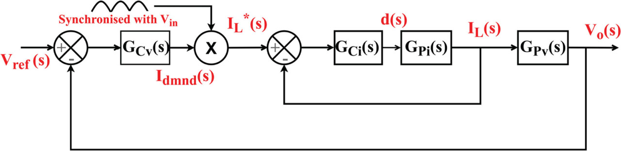
Figure 2.
PFC control block diagram. PFC, power factor correction.
The inner current loop is responsible for making the instantaneous inductor current track the sinusoidal reference supplied by the outer voltage loop. Because this loop directly shapes the input-current waveform, it must act rapidly for changes in the input voltage or load to prevent distortion. Therefore, its operating timescale is closely coupled to the switching action. This makes linearised state space averaging (SSA) an appropriate modelling method for this loop. The resulting small-signal TF describes how small variations in the duty cycle produce changes in the inductor current, forming the required plant model for the inner-loop controller design.
In contrast, the outer voltage loop governs the DC-link voltage by regulating the average input power delivered to the output capacitor. The voltage dynamics are determined by the energy stored in the relatively large-value capacitor, and thus a slower time scale compared to both the switching frequency and the inner-loop bandwidth. Furthermore, to avoid distortion of the input current and degradation of the PF, the voltage-loop bandwidth must be maintained below twice the line frequency. Consequently, a low-frequency averaged model that captures the dominant energy-balance dynamics while neglecting high-frequency switching effects is sufficient and appropriate for outer-loop controller design.
To address this, a FDM strategy is proposed that separates the control design into two distinct frequency domains. The inner current loop is modelled using switching-period SSA, which is appropriate for fast dynamics and small duty-cycle variations. The outer voltage loop is designed using the proposed low-frequency energy-based CCT method, which captures the slow energy dynamics over the line frequency. This separation ensures that each loop is modelled in its natural operating domain, thereby preserving physical accuracy while maintaining analytical simplicity for controller design.
3.1. Inner current-loop modelling via SSA approach
To model the inner current loop, relevant parasitic elements, such as the ESR of the boost inductor rL, on-state resistance of the switch rS, forward resistance of the diode rD, ESR of the capacitor rC, and cut-in voltage of the diode Vγ, are incorporated into the model. A continuous-time linear model is obtained by applying SSA over the switching cycle and linearising it around a steady-state operating point. This standard approach represents the dominant high-frequency dynamics necessary for inner-loop control design.
The inner current loop employs a controller with a bandwidth of approximately one-tenth the switching frequency (5 kHz), ensuring fast current tracking. At this bandwidth, the 50 Hz input voltage can be considered nearly constant within a single switching cycle, which simplifies the dynamic modelling process. The high-speed inner loop then accurately tracks the sinusoidal current reference generated by the outer loop, minimising current errors and providing compensation for input-voltage variations.
The inner-loop SSA TF is derived by averaging over the switching periods. At this timescale, the line frequency variation of the operating point is negligible. At any instant in the line cycle, the instantaneous duty cycle can be treated as a constant from the switching frequency perspective. This is because the inner-loop bandwidth (5 kHz) is 100 times faster than the line frequency (50 Hz). This ensures that the inner loop is fully settled within each increment of the line cycle before the operating point is changed. The resulting inner current control TF (Erickson and Maksimovic, 2007) is expressed as
where , , , d0 = nominal duty ratioThis second-order TF exhibits two conjugate complex poles, indicating potential oscillatory behaviour with damping provided by the effective series resistance reff from the combined parasitic. The right-half-plane zero, which is characteristic of boost converters, introduces a phase lag.
PI controllers are widely used in boost PFC circuits because of their simplicity and ease of implementation. However, they inherently exhibit a finite gain at the fundamental frequency. This results in a steady-state tracking error for sinusoidal references (Kuperman, 2015). Although PR controllers or synchronous frame (dq) transformations can eliminate this error, they introduce significant implementation complexity in single-phase systems.
To analyse the error in sinusoidal current tracking, the parasitic resistances and diode cut-in voltage are neglected. In addition, the numerator is simplified as the term is negligible. Hence, the inner current control TF becomes
This second-order system has a zero at the origin and two conjugate poles. The sinusoidal current reference is given by
In the Laplace domain,
For a unity feedback closed-loop system with controller GCi(s) and plant GPi(s), the feedback is equal to the output IL(s). From the block diagram shown in Figure 3, the error can be derived as
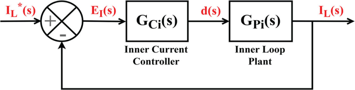
Figure 3.
Inner current control loop in boost PFC systems. PFC, power factor correction.
The term GPi(s) × GCi(s) is the open-loop gain L(s). The magnitude of the steady-state sinusoidal error is found by evaluating EI(s) at s = jωg
When ωn ≠ ωg, the simplified inner current-loop plant TF is given by
The denominator ωn2 − ωg2 is a real non-zero value when ωn ≠ ωg. Therefore, the steady-state error, |Ess| ≠ 0. The finite gain of the PI controller at ωg cannot eliminate this error. A larger proportional gain Kp reduces it but introduces phase margin problems and can destabilise the loop. A resonant controller provides an infinite gain at that frequency and eliminates the error. But the cost and controller complexity increase. This is the fundamental limitation of a PI controller with a sinusoidal reference.
To address this challenge without increasing the control complexity, a novel passive plant-shaping strategy, GART, is proposed. The GART leverages the second-order dynamics of the inner-loop current control plant to enhance the gain at the grid frequency. Rather than modifying the controller structure, it adjusts the converter’s passive components such that the plant itself exhibits a natural resonance aligned with the line frequency, thereby improving the loop gain and reducing the steady-state error.
3.1.1. GART to enhance PI control
The proposed method introduces a passive tuning technique to enhance the frequency response of a plant, which indirectly improves the tracking performance of the standard PI controller. By aligning the natural resonance of the converter with the grid frequency, this approach improves the rejection of disturbances and reduces the THD without increasing the complexity of the controller. GART uses the natural resonance of the inner current-loop plant to boost the effectiveness of the controller. The proposed method involves selecting a capacitor value such that the resonant frequency is aligned with the grid frequency. Based on the small-signal model of the inner loop in Eq. (1), the control-to-current TF exhibits conjugate poles with a natural frequency of
By selecting the output capacitor C such that this resonant frequency aligns with the grid frequency (ωg = 2πfg), the frequency response of the plant is shaped to boost the gain at fg (50 Hz). The optimum value of the capacitor Copt is given by
The DC-link capacitor based on the voltage ripple specifications is given by Gillmor (2016).
The optimised value of the DC-link capacitor obtained from Eq. (9) must satisfy the inequality condition given in Eq. (10). Therefore, combining Eqs (9) and (10), the capacitor design can be given as
Substituting the specifications of the system under consideration, we get
Therefore, the condition given in Eq. (11) is satisfied. For systems with complex impedance loads and tight regulation requirements, such as in this DBD-based ESP application, a significantly larger capacitance is required to stabilise the voltage loop and suppress low-frequency disturbances. This leads to the choice of a 991 μF capacitor (rounded to 1,000 μF using standard component values), not only for energy buffering but also because it satisfies the resonance condition imposed by the GART. Thus, GART offers an optimisation criterion that complements traditional ripple-based sizing. At the same time, this large capacitance slows the voltage dynamics of the system, reinforcing the need for an FDM approach in controller design. Thus, the proposed GART and FDM frameworks assist in passive component selection and loop compensation strategy.
This passive tuning introduces a resonance peak in the Bode response of the plant at the grid frequency. This increases the open-loop gain at the frequency of interest without requiring any modification to the controller itself. As a result, the PI controller, despite lacking infinite gain at 50 Hz, can achieve significantly reduced tracking error and lower THD due to the increased loop gain at the reference frequency. Thus, GART compensates for the limitations of the controller through deliberate plant design. Thereby, preserving the simplicity and robustness of PI-based architectures while enhancing performance to a level comparable with more complex control schemes.
The steady-state tracking problem at the grid frequency, which requires PR controllers or synchronous frame PI, is completely solved by GART at the plant level. With ωn = ωg, the plant provides an infinite gain at ωg. Hence, the controller does not need to provide infinite gain at ωg (the plant handles this issue). Therefore, the only function of the controller is to make the current track the sinusoidal reference.
3.1.1.1. Sensitivity of GART to the time-varying duty cycle
In single-phase boost PFCs, the continuously varying instantaneous duty cycle d(t) causes the plant’s natural frequency ωn(t) to sweep dynamically across the grid half-cycle. Therefore, the strict GART condition (ωn = 50 Hz) is intentionally aligned specifically at the peak of the AC mains (θ = 90°), where maximum power transfer and highest tracking errors occur. While exact resonance decays near the zero-crossings, the plant’s inherent damping provides a wide high-gain bandwidth (e.g. a 16 Hz -3 dB window). This ensures that the plant mathematically delivers a highly supportive gain (≥70% of peak capability) over a broad, continuous window (approximately 65°) perfectly centred over the AC crest. The practical effectiveness of this peak-aligned optimisation is inherently validated by full non-linear switching simulations, which naturally incorporate this frequency sweep and successfully achieve optimal THD minimisation.
3.1.1.2. Trade-offs of GART: Volume, cost, and control simplicity
It should be noted that the proposed GART methodology is not intended to maximise the converter power density but rather represents an application-specific optimisation that deliberately trades an increased DC-link capacitance for enhanced low-frequency energy buffering, improved decoupling from the non-linear DBD load, and simplified PI-based controller implementation. Compared with the conventional ripple-based design requirement of 358 μF (≈400 μF practical value), the proposed 1,000 μF DC-link capacitor provides improved energy storage capability and reduced double-line-frequency voltage ripple at the expense of increased physical volume and a modest increase in component cost. Although film-based DC-link solutions offer superior reliability, self-healing capability, and ultra-low ESR, they typically employ significantly lower capacitance values and often rely on advanced control to maintain dynamic performance in the presence of a larger 100 Hz bus-voltage ripple. Furthermore, capacitance values of several 100 μF to approximately 1,000 μF are frequently encountered in practical single-phase PFC systems for energy buffering and hold-up requirements. Therefore, the proposed GART approach intentionally exploits a larger energy buffer to achieve improved low-frequency decoupling and control simplicity, making it particularly suitable for cost-sensitive HV power supplies employing non-linear DBD loads.
3.1.2. Inner current-loop controller design
To ensure reference tracking and minimal THD for active PFC, the inner current loop must be designed with a high bandwidth (5 kHz) to decouple its fast dynamics from the slower outer voltage loop. Rather than employing the traditional frequency-domain Barkhausen criteria or K-factor method (Venable, 1983), which often necessitates iterative trial-and-error tuning and a Bode stability criterion check to secure adequate phase margins, this design utilises a direct approach based on the DTTP. For the controller design, the controller structure is not prescribed a priori; rather, the desired characteristics of the current response are defined. The reference current is given by
where Iref = Idmnd sin(ωgt) is the desired amplitude input sine reference and u(t) is the Heaviside unit step function. An ideal step response can be represented by a first-order exponential response y(t) =1 − e−ωcit characterised by the time constant ωci−1. The desired closed-loop response to a step change in the current reference is given asIn the Laplace domain,
The desired closed-loop TF is given by
For a unity feedback system, with plant TF GPi(s) and controller TF GCi(s), the closed-loop TF is given by
From Eq. (18), the loop gain can be given as
From Eqs (19) and (2), the required controller structure is obtained as
When ωn = ωg,
Expanding Eq. (21) results in a standard PI controller, , where the tuning coefficients are defined by the physical plant parameters and the desired bandwidth.
The proportional gain for the inner current loop
The integral gain for the inner current loop
To evaluate the effectiveness of the proposed DTTP tuning algorithm, the closed-loop step response of the inner current loop is compared with that of a conventional PI controller design, as shown in Figure 4. The conventional design utilises the traditional frequency-domain approach based on the Barkhausen stability criterion, which is tuned for a 45°phase margin. To ensure a rigorous comparative analysis, both controllers were applied to the exact same plant model and evaluated under identical operating conditions and passive component values. The conventionally tuned PI achieves a fast rise time of 36.9 μs but exhibits a relatively high overshoot of 34.4% and a settling time of 289 μs. In contrast, the controller tuned using the proposed method significantly improves the transient behaviour, reducing the overshoot to 13.4% while shortening the rise time to 23.2 μs and the settling time to 171 μs. The reduced peak excursion and faster settling confirm that the proposed tuning provides better damping and transient robustness for the current loop.
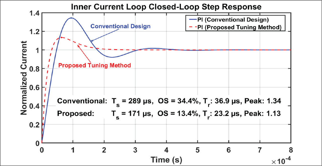
Figure 4.
Closed-loop step responses of the inner current loop with different PI tuning methods. Ts: Settling time, OS: overshoot, Tr: rise time. PI, proportional integral.
3.2. Outer voltage-loop modelling via CCT approach
For the boost PFC converter, the outer voltage loop operates at a significantly lower bandwidth (5 Hz) than the inner current loop (5 kHz) in order to ensure decoupling. This wide separation of time scales allows simplified modelling approaches that focus exclusively on low-frequency energy dynamics, eliminating the high-frequency switching behaviour.
In the proposed CCT approach, the outer voltage loop is modelled by directly relating the capacitor charging current to output-voltage variations. As shown in Figure 5, the converter is simplified to a low-frequency equivalent circuit based on the power balance (Basso, 2008). The PFC power stage can be considered as an equivalent averaged current source supplying the output capacitor and load. Unlike double-averaged or energy-based models, the CCT formulation directly derives capacitor dynamics from first principles. The principle of this approach is that the output-voltage variations in the boost converter are governed by charging current into the output capacitor (iC). This net current represents the difference between the charging current supplied by the inductor through the diode (iD) and that drawn by the load (io). For a boost converter, the governing relationship can be expressed as
where iD(t) is the charging current supplied to the capacitor by the inductor through the diode and io(t) is the current drawn by the load. For a resistive load, , where Ro is the load resistance. The charging current in a boost converter (diode current) is directly related to the inductor current (iL(t)) and duty cycle by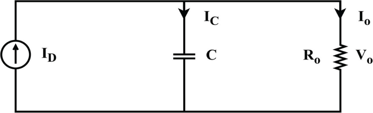
Figure 5.
Simplified equivalent circuit diagram of boost PFC based on average power. PFC, power factor correction.
Given the low bandwidth of the outer loop (5 Hz), the duty cycle d(t), which varies at line frequency, can be approximated by its average duty cycle D over one half cycle. The instantaneous duty cycle is determined by the volt-second balance condition on the boost inductor and is given by
where Vin,pk is the peak amplitude of the rectified supply voltage and Vo is the regulated output DC voltage. The average over one half cycle givesFrom the perspective of such a low-bandwidth system, these high-frequency variations appear as their average values. This time-scale separation principle forms a mathematical foundation that enables the simplified capacitor-charge approach to accurately capture the relevant dynamics for the outer voltage-loop design, despite the inherently time-varying nature of the PFC converter. Substituting the averaged duty cycle yields the simplified large-signal dynamic equation:
To derive an LTI TF, the large-signal non-linear equation must be linearised around the steady-state DC operating point (VoO ,ILo). Let f(vo,iL) denote the non-linear function governing the capacitor current in terms of the state variables vo and iL.
Small-signal perturbations are introduced around the operating point such that
Applying a first-order Taylor series expansion about (VoO, ILO) and evaluating the partial derivatives of f(vo, iL) with respect to the state variables at the steady-state equilibrium point yields the linearised small-signal differential equation for the outer voltage loop.
Then taking the Laplace transform and solving for the small-signal TF from inductor current to output voltage gives the following:
This first-order TF has a DC gain of (1−D)Ro/2 and a pole at , capturing the slow voltage-loop dynamics. The CCT approach can be applied to a wide range of load conditions, including constant resistance, constant power, constant current, and high impedance types. It provides a unified framework for analysing the output-voltage dynamics of boost PFC converters. This method is both simple and physically intuitive, as it directly links the capacitor charging current to the output voltage.
3.2.1. Outer voltage-loop controller design
Similar to the inner current-loop design, a direct approach based on the DTTP is used for the outer voltage-loop design. The structure of the outer voltage control loop is shown in Figure 6. The desired closed-loop response to a step change in the voltage reference is given by
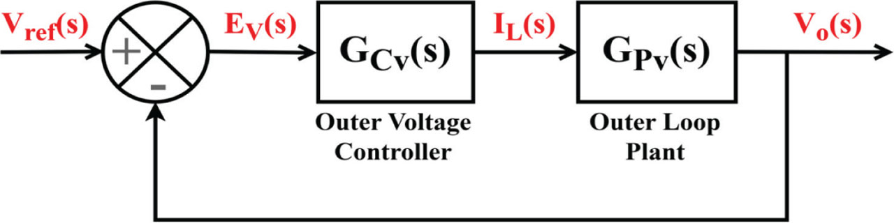
Figure 6.
Outer voltage control loop in boost PFC systems. PFC, power factor correction.
In the Laplace domain, this is expressed as
The desired closed-loop TF T(s) is
For a unity feedback system with loop gain L(s) = GCv(s) × GPv(s), the closed-loop TF is
From the above equation, the required loop gain L(s) is derived as
To achieve this loop gain, the controller Gcv(s) must satisfy
Expanding this equation yields a standard PI controller, , where the tuning coefficients are defined by
To evaluate the effectiveness of the proposed DTTP tuning algorithm, the closed-loop step response of the outer voltage loop is compared with that of a conventional PI controller design, as shown in Figure 7. The conventional design utilises the traditional frequency-domain approach based on the Barkhausen stability criterion, which is tuned for a 70° phase margin. To ensure a rigorous comparative analysis, both controllers are applied to the exact same plant model and are evaluated under identical operating conditions and passive component values. The two controllers show very similar dynamic performances. The conventionally tuned PI exhibits a rise time of 45.7 ms, a settling time of 0.22 s, and an overshoot of 13.6%, while the proposed tuning yields a slightly faster rise time of 43.4 ms, a settling time of 0.218 s, and a reduced overshoot of 11.4%. The differences between the two responses are modest. Both designs satisfy the desired bandwidth and damping requirements for the outer loop. This behaviour confirms that, unlike the inner current loop, the outer voltage-loop dynamics are less sensitive to the specific PI tuning method due to the dominant first-order nature of the plant.
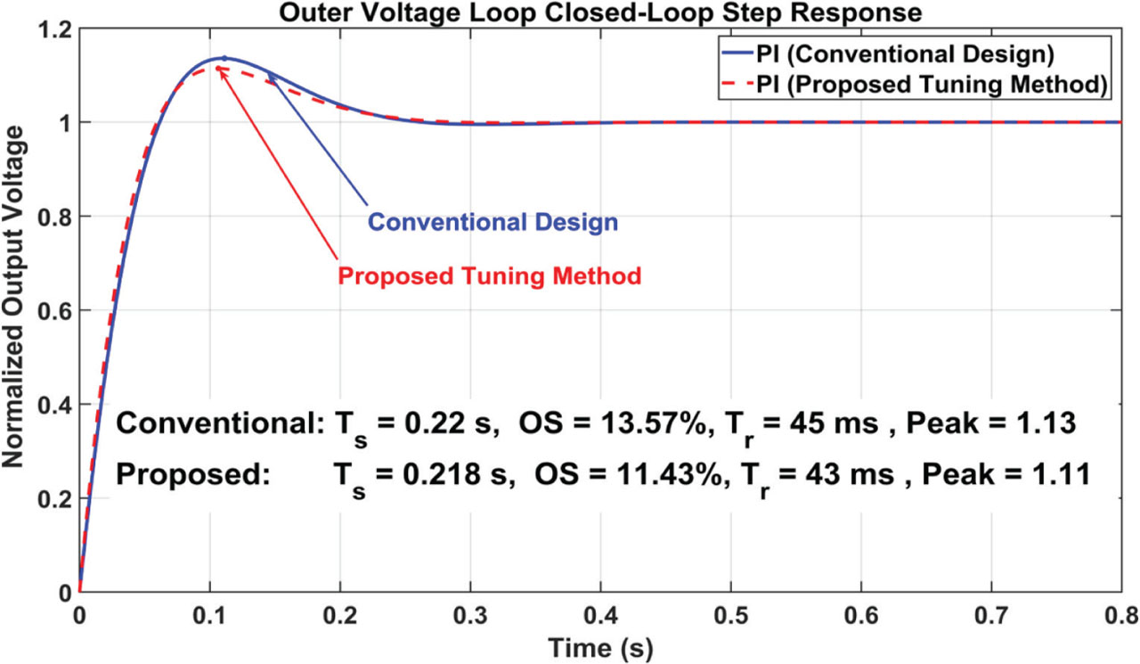
Figure 7.
Closed-loop step responses of the outer voltage loop with different PI tuning methods. Ts: Settling time, OS: overshoot, Tr: rise time. PI, proportional integral.
4. Generalised PI controller design algorithm
The control architecture of the boost PFC converter with dual-loop regulation is shown in Figure 8. The control structure uses PI controllers. A notable property of the proposed design framework is that the PI controller gains for both loops are expressed entirely in terms of the converter’s passive component values, operating point, and designer-specified closed-loop bandwidth. This establishes a direct analytical link between the power stage and controller designs. This eliminates the need for iterative frequency-domain tuning and enables the complete controller to be derived immediately after passive component sizing. Hence, a generalised algorithm can be framed for this framework for the boost PFC design.
Input the Specifications of the Converter
Define the system requirements: Output power Po, input voltage Vin, output voltage Vo, switching frequency fs, current ripple ΔIL, voltage ripple ΔVo, and efficiency η.
Sizing of the Passive Components
Compute the inductance L, load resistance Ro, nominal duty cycle d0, and average duty cycle D.
Bandwidth Selection
Select the inner- and outer-loop controller bandwidths according to the frequency separation principle
where fi is the current-loop bandwidth and fv is the voltage-loop bandwidth. A good choice is to take the outer-loop bandwidth between and and inner-loop bandwidth as .Capacitor Selection through GART
Compute the optimal capacitance Copt and verify that the ripple constraints are satisfied
PI Controller Design
Calculate the proportional (Kp) and integral (Ki) gains for both control loops
Inner Current Loop
Outer Voltage Loop
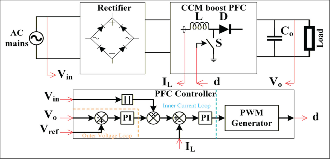
Figure 8.
Control architecture of boost PFC converter with dual-loop regulation. PFC, power factor correction; PI, proportional integral.
The proposed design procedure provides a systematic framework for the selection of passive components and the tuning of a dual-loop control architecture for a boost PFC. By applying the FDM approach, a clear separation between the high-bandwidth inner current loop (fi) and the lower-bandwidth outer voltage loop (fv) is maintained, ensuring system stability and decoupling. The derivation of the PI controller gains, Kpi, Kii for current tracking and Kpv, Kiv for voltage regulation, directly links the physical plant parameters (L, C, Ro) to the desired closed-loop performance. Furthermore, the integration of the GART-based capacitor selection ensures that the optimal capacitance Copt not only satisfies steady-state ripple constraints but also aligns with the dynamic requirements of the system. This design approach ensures robust tracking of the current reference and precise regulation of the output voltage. Here, the inner current-loop crossover frequency is selected as 5 kHz, and the outer voltage-loop crossover frequency is restricted to 5 Hz.
In boost PFC converters, the outer voltage loop uses PI control since voltage dynamics are dominated by the output capacitor and load, enabling effective low-order plant compensation. Most implementations use PI control for voltage regulation regardless of current control strategy. In contrast, the inner current loop must accurately track a sinusoidal reference over the line cycle, and conventional PI control introduces tracking errors (Israr and Samuel, 2024; Zmood and Holmes, 2003). This led to the development of alternative current control strategies, such as PR, hysteresis, deadbeat (DB), model predictive, model-free and sliding mode controls (Kazmierkowski and Malesani, 2002; Quiroga et al., 2025).
To evaluate the effectiveness of the proposed inner-loop PI design, a comparative performance analysis is conducted with major current control strategies reported in the literature, while maintaining a PI controller for the outer voltage loop in all cases. Table 2 presents a qualitative comparison between the proposed controller and major control strategies for boost PFC converters in terms of computational and implementation aspects, dynamic response, and steady-state performance. Furthermore, to substantiate this with quantitative benchmarks, Table 3 summarises the real statistical parameters, including experimental hardware specifications, output capacitance, nominal THD, and PF, extracted directly from the cited literature. The performance metrics for the alternative control strategies are extracted from the experimental and simulation benchmarks reported in the cited literature, whereas the parameters for the proposed FDM-GART method are obtained directly from our experimental prototype.
Table 2.
Qualitative comparative performance of inner current control strategies for boost PFC converters.
| Performance parameter | PI | PR | HCC | DB | MPC | MFPC | SMC | Proposed PI |
|---|---|---|---|---|---|---|---|---|
| Computational and implementation aspects | ||||||||
| Computational burden (per cycle) | L | M | L | H | VH | M | M | L |
| Implementation complexity | L | M | L | H | VH | M | H | L |
| Parameter sensitivity | M | M | L | VH | H | L | VL | M |
| Dynamic performance | ||||||||
| Current transient response | S | F | VF | VF | VF | F | F | S |
| Phase error (grid frequency) | NZ | Z | NrZ | Z | NrZ | NrZ | Z | NrZ |
| Steady-state performance | ||||||||
| Steady-state current THD | >5% | <5% | <3% | <5% | <2% | <5% | <3% | <5% |
| Steady-state error | NZ | Z | NrZ | Z | NrZ | NrZ | Z | NrZ |
[i] DB, deadbeat; F, fast; H, high; HCC, hysteresis current control; L, low; M, moderate; MFPC, model-free predictive control; MPC, model predictive control; NrZ, near zero; NZ, non-zero; PI, proportional integral; PR, proportional resonant; S, slow; SMC, sliding mode control; VF, very fast; VH, very high; Z, zero.
Table 3.
Experimental hardware specifications and statistical performance parameters of the compared control strategies.
| Control strategy (references) | Rated power (W) | Vin/Vout (V) | Output capacitor (μF) | Switching frequency (kHz) | THD (%) | PF |
|---|---|---|---|---|---|---|
| PI: Okilly and Baek (2022) | 2,000 | 220/400 | 950 | 100 | 5.5 | 0.9935 |
| PR: Liu et al. (2013) | 3,000 | 220/400 | 940 | 19.2 | N.R | N.R |
| HCC: Shehata et al. (2023) | 100 | 40/100 | 1,000 | 21 | 2.61 | 0.999 |
| DB: Mattavelli et al. (2005) | 400 | 230/400 | 330 | 50 | N.R | N.R |
| MPC: Israr and Samuel (2025) | 500 | 220/400 | 100 | 20 | 1.8 | 0.999 |
| MFPC: Gu et al. (2021) | 1,000 | 110/300 | 990 | 50 | N.R | 0.99 |
| SMC: Mohanty and Panda (2016) | 500 | 230/390 | 470 | 200 | 2.4 | 0.999 |
| Proposed work (FDM-GART PI) | 900 | 230/400 | 1,000 | 50 | 4.7 | 0.999 |
[i] N.R. = Not explicitly reported in the text.DB, deadbeat; FDM, frequency-differentiated modelling; GART, grid-aligned resonance tuning; HCC, hysteresis current control; MFPC, model-free predictive control; MPC, model predictive control; PF, power factor; PI, proportional integral; PR, proportional resonant; SMC, sliding mode control; THD, total harmonic distortion.
The PI controller is the simplest to implement but cannot eliminate steady-state tracking error at 50 Hz because the integrator provides an infinite gain only at DC. The resulting phase error directly degrades the PF, making the PI unsuitable for the PFC without further correction (Okilly and Baek, 2022). The PR controller corrects this through a resonant term tuned to the grid frequency, achieving near-zero steady-state and phase errors; however, the resonant gain must remain at the actual grid frequency, which shifts under load and requires a phase-locked loop (PLL) (Liu et al., 2013; Parvez et al., 2020; Teodorescu et al., 2006). Hysteresis current control (HCC) has the fastest response time; however, its variable switching frequency complicates the electromagnetic interference filter design (Kazmierkowski and Malesani, 2002; Shehata et al., 2023). Both DB and MPC deliver fast dynamics and low THD. DB is highly sensitive to inductance variation (Mattavelli et al., 2005), whereas MPC has the highest hardware requirement, and its cost function has no systematic design method (Israr and Samuel, 2025; Kouro et al., 2008). Model-free predictive control (MFPC) and SMC offer the best robustness against load uncertainties but similarly require complex algebraic estimators or Lyapunov stability analysis and boundary layer design, thereby adding considerable design effort (Gu et al., 2021; Mohanty and Panda, 2016; Tan et al., 2008). The proposed FDM-GART PI method combines near-zero steady-state and phase errors with the simplicity of PI, requiring no PLL. The trade-off for this low computational burden is a larger output capacitance (1,000 μF) and a PR-comparable transient response, although Table 3 demonstrates that this capacitor sizing aligns well with recent advanced hardware prototypes. Although non-linear controllers offer faster dynamics at the expense of intensive computational complexity, the proposed design achieves highly competitive power quality (4.7% THD, 0.999 PF) with minimal implementation effort, providing a cost-effective and reliable solution for HV applications.
5. Simulation Results and Discussions
This section presents the simulation results used to evaluate the effectiveness of the proposed control strategy for the CCM boost PFC converter. The first subsection examines the influence of variations in the supply voltage, supply frequency, capacitance, and parasitic elements on the performance of the GART approach. The second subsection evaluates the steady-state and transient performances of the system under different operating conditions. All simulations are performed using MATLAB/Simulink.
5.1. Validation of GART: Harmonic performance, dynamic response, and robustness
This section validates the effectiveness of the proposed GART strategy by demonstrating how the selection of a single output capacitance of approximately 991 μF (rounded to 1,000 μF) simultaneously minimises the transient THD and preserves the fast dynamic response in a CCM boost PFC converter operating under a simple PI controller.
5.1.1. Robustness and stability under parameter variations
When the output capacitance is set to 1,000 μF (with the corresponding reff ≈ 0.7 Ω), the 3-dB bandwidth of the open-loop plant inner current loop Gpi(s) is observed to be approximately 105 rad/s (≈ 16 Hz), as shown in Figure 9. According to the Central Electricity Authority of India, frequency deviations of the grid of ±0.5 Hz are allowed, with emergency load shedding triggered below 49.2 Hz (i.e., ≈ a deviation of 1 Hz). Because this ±1 Hz remains well within the 16 Hz control bandwidth, the loop gain at 50 Hz remains essentially unaffected. Furthermore, ±10% of the voltage variations in the grid correspond to a duty cycle shift of only approximately 0.04, which has a negligible effect on the resonant frequency. Thus, under all standard grid conditions, the resonance remains within the loop bandwidth and continues to enhance performance without degradation.
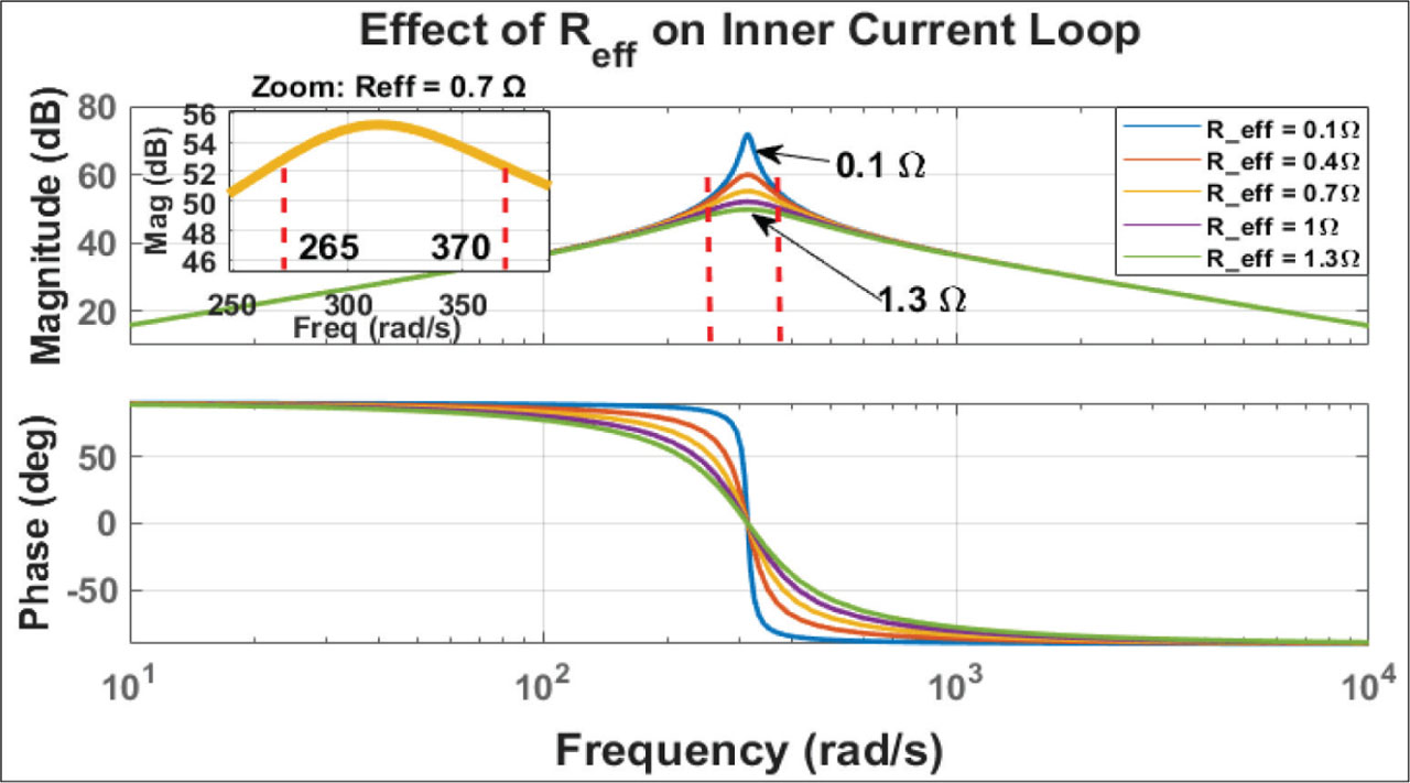
Figure 9.
Bode analysis of the effect of Reff on the inner current loop.
With a fixed capacitance of 1,000 μF, Figure 9 also shows the effect of varying Reff, which is governed by rc, rL, rs, and rD. Increasing Reff increases the damping ratio , which flattens the resonant peak and widens the bandwidth. Low Reff values (e.g., 0.3 Ω) lead to pronounced gain peaking near 314 rad/s, ideal for harmonic rejection, but with reduced stability margins. A moderate Reff (≈ 0.5 Ω) balances gain and damping, suppressing the 100 Hz ripple while maintaining robust inner-loop behaviour. Because the resonance location is fixed by the chosen capacitance, the ESR provides a convenient design handle for shape damping without affecting ωn.
Although the passive damping ratio for C = 1,000 μF and minimal ESR is underdamped (ζ ≈ 0.2), the overall stability of the system is ensured by active damping from the inner PI controller (bandwidth = 5 kHz) and the outer voltage-loop PI controller (bandwidth = 5 Hz). The inner loop mitigates LC oscillations, while the outer loop suppresses residual 100 Hz ripple, ensuring full regulation even with lightly damped passive elements. Time-domain simulations further confirm this: the 991 μF case damps out oscillations by 0.5 s and achieves THD approximately 2%, while the 2,200 μF case requires 1.2 s to settle. The 470 μF case settles quickly (<0.4 s) but exhibits persistent 100 Hz ripple and elevated THD (3.7%).
Figure 10 shows the Bode plots of the inner current loop of the plant for capacitance values of 470, 680 μF, 991 μF, 1,000 μF, 1,500 μF and 2,200 μF. As capacitance increases, the natural resonant frequency decreases. For C < 991 μF, the resonant frequency exceeds 314 rad/s (grid frequency), resulting in a suboptimal gain at 50 Hz. At 991–1,000 μF, the resonance aligns with 314 rad/s, maximising the gain at the grid frequency, which is the central premise of the GART. For larger capacitances, ωn shifts below 314 rad/s, reducing the gain at the fundamental frequency.
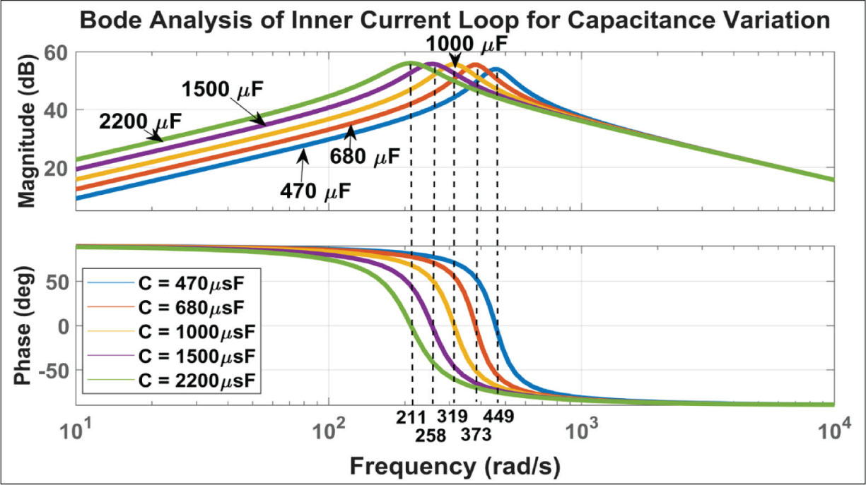
Figure 10.
Bode analysis of inner current loop for capacitor variations.
Interestingly, while the resonant frequency shifts significantly with C, the peak magnitude remains relatively constant across this range, indicating that the damping is not strongly affected by capacitance alone. Similarly, although the phase plot shifts to lower frequencies as C increases, the overall phase margin remains largely unchanged. These observations confirm that the output capacitance mainly tunes the resonance location without affecting damping or phase margin, unless it is accompanied by changes in Reff. This confirms the fundamental assumption of GART: the output capacitor can be used to align the resonant peak of the plant with the grid frequency, thereby maximising the gain at 50 Hz and reducing the THD without sacrificing loop stability. These characteristics make GART a robust design tool that uses plant dynamics instead of complex control.
5.1.2. Dynamic response and harmonic performance evaluation
Figure 11 presents the simulation results for THD and the settling time at various capacitance values. At 470 μF, the system exhibits fast settling (0.40 s) but an increase in THD (3.7%). As the capacitance increases to 991 μF, the THD drops to 2.1% while maintaining a reasonable settling time of 0.55 s. However, beyond 1,000 μF, the settling time increases significantly: 0.90 s at 1,500 μF, 1.20 s at 2,200 μF, and up to 3.00 s at 4,700 μF. Thus, the 991–1,000 μF range represents a sweet spot, minimising THD while preserving dynamic response. This strongly supports the core premise of the GART that tuning the natural resonance of the plant to match the frequency of the grid delivers the best trade-off between harmonic suppression and regulation speed.
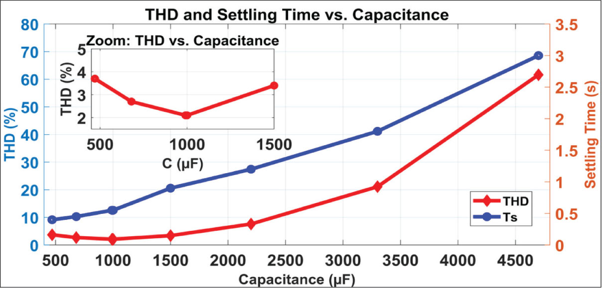
Figure 11.
Combined plot of THD and settling time versus output capacitance. THD, total harmonic distortion.
In short, GART removes the conventional trade-off between THD reduction and dynamic response. By choosing 1,000 μF, the resonance of the inner loop is aligned with the grid, resulting in minimal transient distortion under a simple PI architecture. At the same time, the settling time remains less than 0.5 s, much better than the multiple seconds required by large capacitance filtering methods. Adjusting the capacitor ESR (or adding a small series resistor) further ensures adequate damping and a phase margin without shifting the resonance. This combination of resonance-based passive tuning and active PI control delivers high power quality and rapid voltage regulation in a compact, cost-effective boost PFC design.
5.2. Steady-state and dynamic performance
To validate the proposed modelling and control strategy prior to hardware implementation, detailed simulations are carried out in MATLAB Simulink R2024b (The MathWorks, Inc). The model incorporated complete inner and outer control loops with PI compensators and included all relevant parasitic elements to closely reflect the physical system. The simulation parameters are shown in Table 4.
Table 4.
Simulation parameters.
| Parameters | Value | Parameters | Value |
|---|---|---|---|
| Output capacitor | 1,000 µF | Switch on-resistance | 0.25 Ω |
| ESR of capacitor | 0.1076 Ω | Forward resistance of diode | 0.03 Ω |
| Resistance of the inductor | 0.5 Ω | Diode cut-in voltage | 1.05V |
Figure 12 shows the steady-state operation of the Boost PFC converter under nominal load conditions. The output voltage settles at the regulated value of 400V, and the output current corresponds to the rated load condition. Figure 12b provides a zoomed-in view, highlighting that the current waveform follows the input voltage, validating the efficacy of the inner current-loop control. The measured steady-state output-voltage ripple (ΔV) is approximately 8V, and the inductor current ripple (ΔI) is approximately 0.04 A. Figure 12c shows the harmonic analysis of the input current, revealing a THD of 1.82%, demonstrating excellent power quality performance. The output voltage settles within 250 ms, indicating a fast dynamic response.
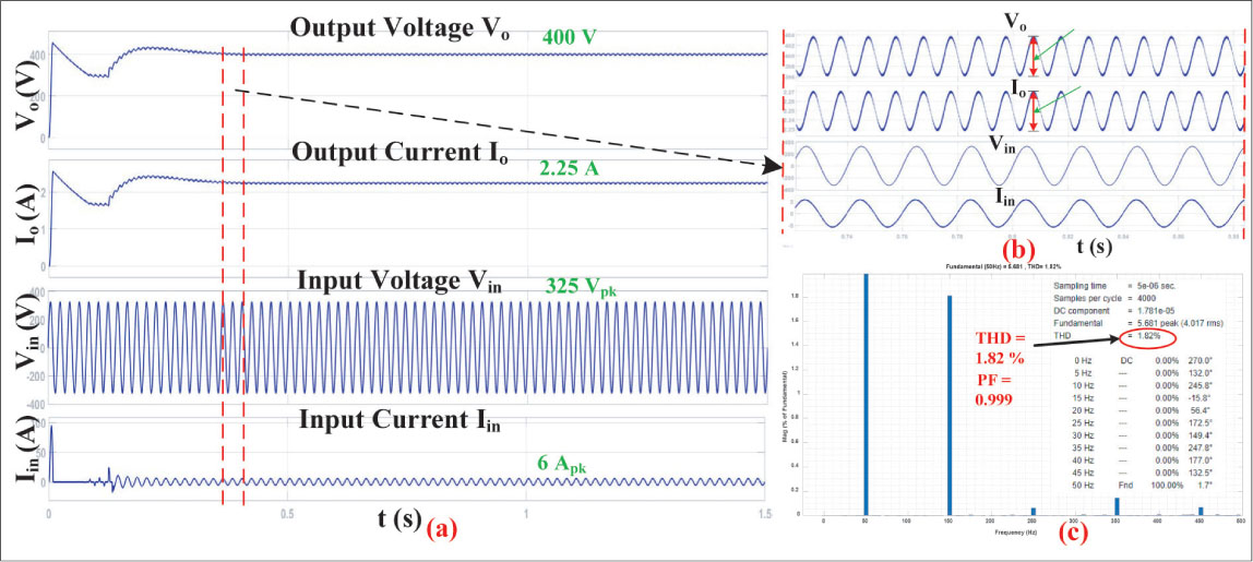
Figure 12.
(a) Steady-state operation of boost PFC under rated load conditions; (b) Zoomed-in waveform showing input current tracking input-voltage and output-voltage ripple; (c) THD of input current. PFC, power factor correction; THD, total harmonic distortion.
Figure 13 illustrates the load regulation performance of the system. The load current is varied in steps from 1.6 A to 2.9 A and then to 4.2 A and then back to 2.9 A, with each transition occurring at 5 s intervals. The outer voltage loop maintains the output voltage regulated at 400 V throughout the load changes. The zoomed-in view of the 5 s transition from 1.6 A to 2.9 A shows a voltage settling time of approximately 250 ms, confirming the robustness of the control system against load disturbances.
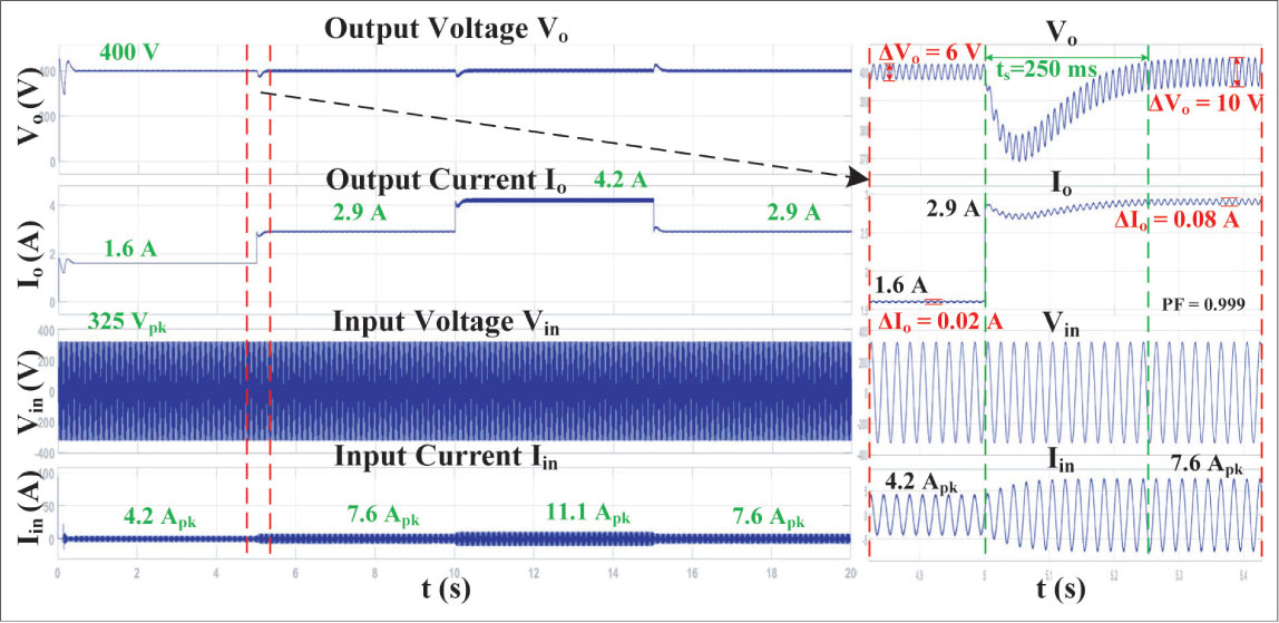
Figure 13.
Load regulation performance of boost PFC converter. PFC, power factor correction.
Figure 14 shows the line regulation performance of the Boost PFC converter. The input voltage is varied in steps from 360Vpk to 400Vpk, then decreased to 320Vpk and 280Vpk, before returning to 350Vpk, with changes introduced every 3 s. The outer loop successfully maintains the output voltage at 400V despite the input-voltage fluctuations. The zoomed-in view around the 15 s mark, during the step from 280Vpk to 350Vpk, shows a voltage settling time of approximately 250 ms. These results confirm that the designed control loops maintain output regulation and effectively suppress input disturbances.
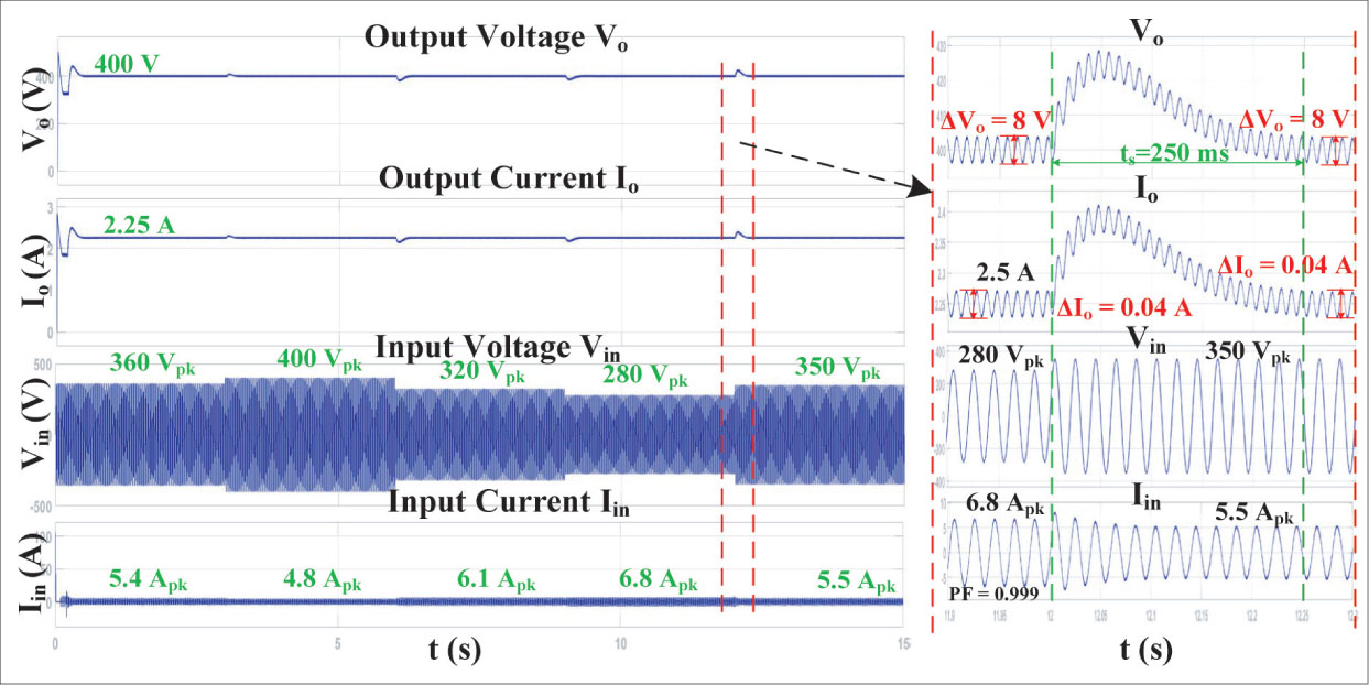
Figure 14.
Line regulation performance of boost PFC converter. PFC, power factor correction.
Overall, the simulation results validate the accuracy of the proposed model and the effectiveness of the controller design in achieving a fast-dynamic response, high PF, and low THD under steady-state and dynamic conditions.
6. Experimental Results
To validate the performance of the proposed CCM boost PFC converter with closed-loop control, a 900 W offline boost power supply is developed and tested. The experimental setup is shown in Figure 15. The hardware prototype is based on a Spartan-6 XC6SLX25 Field-Programmable Gate Array (FPGA) (AMD/Xilinx) (FTG256 package), which implements the PFC control algorithm and PI controllers to generate the Pulse-Width Modulation (PWM) signals required to drive the boost converter switch. Voltage and current feedback signals are acquired through a dedicated signal conditioning and sensor module and fed into the FPGA for real-time control. The measurement system included a three-channel voltage sensor (rated at 600V) and a three-channel current sensor (rated at 55 A). Conditioned analogue signals are digitised using a dual-channel ADC (AD7367), which directly interfaces with the FPGA. The PWM outputs from the controller are routed through a high-speed optically isolated gate driver (FOD3180) to control the boost converter power Metal-Oxide-Semiconductor Field-Effect Transistor (MOSFET). The key instruments used during the testing included a Rohde & Schwarz (Rohde & Schwarz GmbH & Co. KG, Munich, Germany) RTM3004 digital oscilloscope, Fluke 43 B power quality analyser for THD measurements, Teledyne Test Tools T3CP500-5 (Teledyne LeCroy) current probe (5 MHz bandwidth), and Tektronix (Tektronix, Inc., Beaverton, OR, USA) P5200A HV differential probe (50 MHz bandwidth). A 1.5 kW three-phase resistive load bank is employed for load regulation and dynamic performance testing.
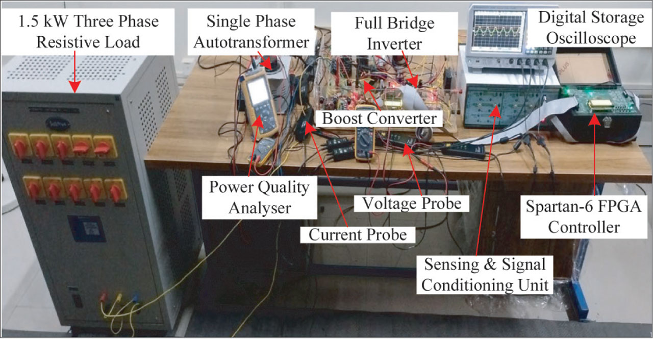
Figure 15.
Experimental hardware setup of the 900 W boost PFC prototype. PFC, power factor correction.
To test how the system responds to the transient, a step change in the reference voltage to 400V is applied. The output-voltage waveform showed a smooth transition with minimal overshoot. From the waveform, the settling time is 300 ms, and the peak overshoot is 12%. These results show that the voltage loop works well and does not cause too much oscillation. The controller followed the reference voltage with minimal deviations. The output-voltage ripple is maintained at 5V, which is in agreement with the expected filtering performance of the capacitor used in the DC link. Furthermore, the average DC output current remains at 2.25 A, matching the design expectations. Figure 16 shows the step response waveform.
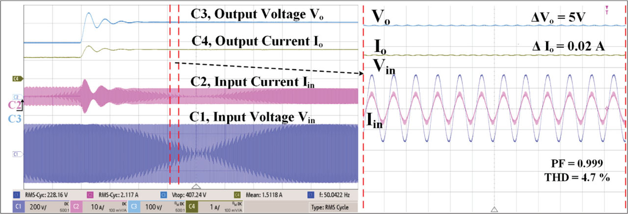
Figure 16.
Input voltage Vin (C1: 200V/div), input current Iin (C2: 10 A/div), output current Io (C4: 1 A/div), output voltage Vo (C3: 100V/div). PF, power factor; THD, total harmonic distortion.
To assess the system’s ability to maintain a stable output voltage under varying loads, the load resistance is varied in discrete steps. The measured output voltage remained within 400 V ± 2 V, indicating excellent load regulation. This confirms that the control system successfully compensated for the load changes without introducing significant transients. The load regulation waveform is shown in Figure 17. It should be noted that while the prototype was designed for a nominal 900 W average load, the high currents were intentionally induced by approximately two times the rated power step-change. As verified by macroscopic switched-RC plasma simulations, this massive step change serves as a mathematically rigorous physical emulation of the extreme, worst-case power surges demanded during abrupt plasma ignition or dielectric breakdown events. The successful containment of these transient overcurrents validates the robust decoupled stability of the proposed FDM-GART control architecture under realistic plasma inception conditions.
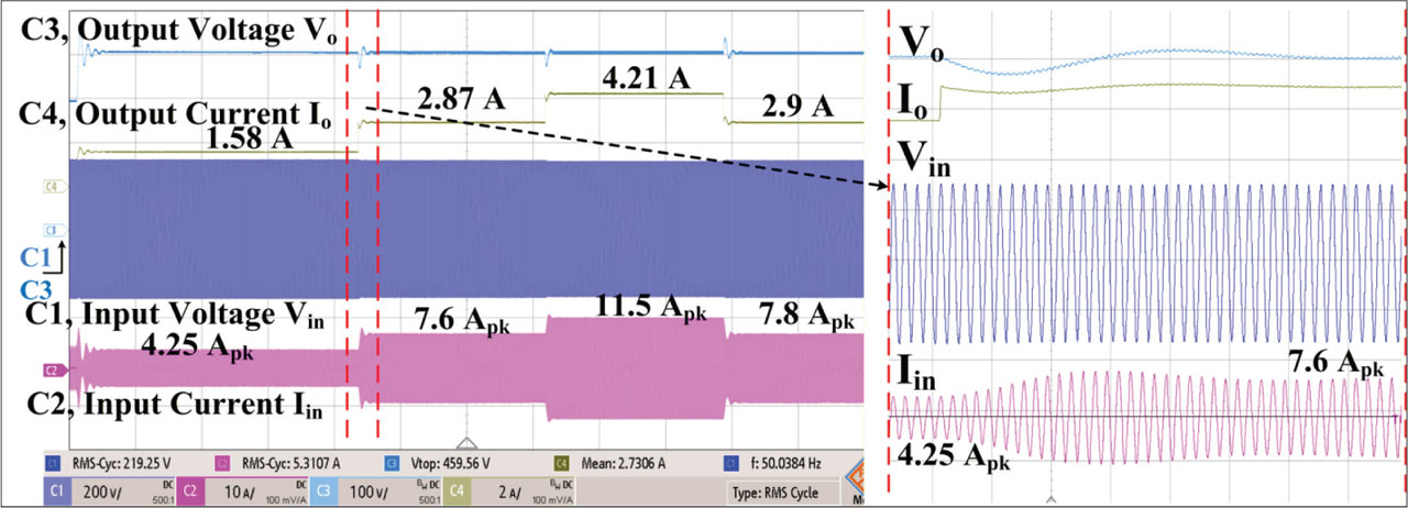
Figure 17.
Load regulation performance of boost PFC converter. Input voltage Vin (C1: 200V/div), input current Iin (C2: 10 A/div), output current Io (C4: 2 A/div), output voltage Vo (C3: 100V/div). PFC, power factor correction.
To test how well the controller could handle changes in the supply, the input voltage is varied in steps while maintaining a constant load. Despite these variations, the output voltage remained regulated at 400 V ± 2 V, which shows that the control strategy is able to reduce line disturbances. The closed-loop compensator ensured that input variations are rejected correctly, thereby maintaining system stability. The results confirm that the voltage remains well-regulated at 400V; the settling time for input variations is 300 ms, and the input current remains sinusoidal without significant distortion. Figure 18 shows waveforms for line regulation.
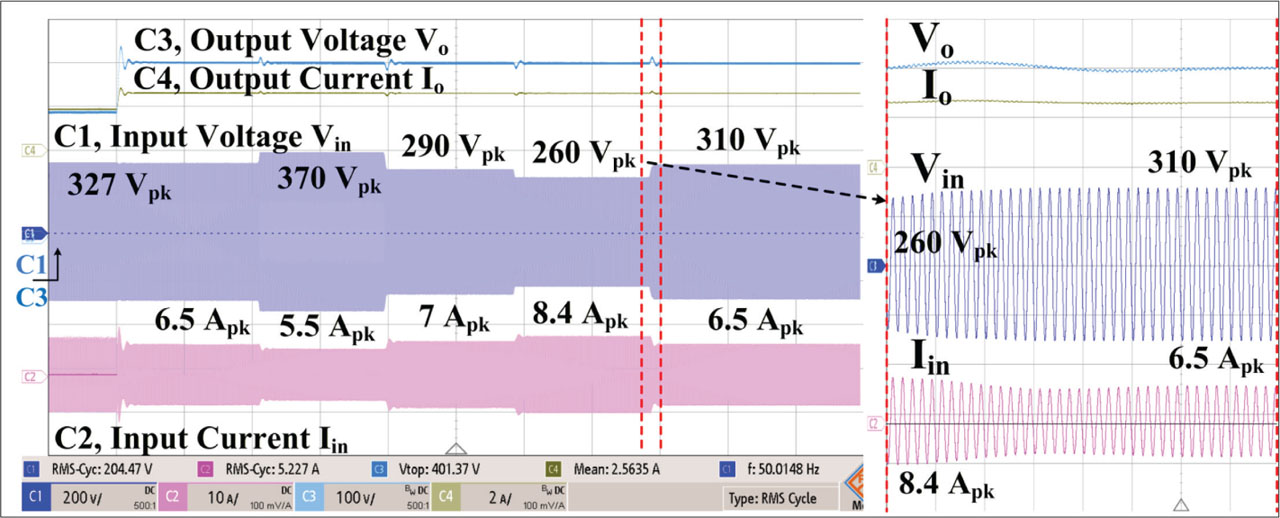
Figure 18.
Line regulation performance of boost PFC converter. Input voltage Vin (C1: 200V/div), input current Iin (C2: 10 A/div), output current Io (C4: 2 A/div), output voltage Vo (C3: 100V/div). PFC, power factor correction.
To further validate the dynamic performance of the proposed digital control system, the input-current and -voltage waveforms are measured before and after enabling the PFC algorithm. As shown in Figure 19, the input-current transitions from a highly distorted shape to a smooth sinusoidal waveform that closely tracks the input voltage within two-to-three-line cycles. This rapid response demonstrates the effectiveness of the implemented PI controllers in enforcing the PFC. The corresponding THD measurement obtained using the Fluke 43 B power quality analyser confirmed a low THD of approximately 4.7%, highlighting the real-time capability of the algorithm to suppress harmonics and shape the input current. These results provide strong experimental validation of the proposed FDM approach and the efficacy of the designed control.
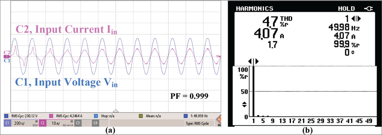
Figure 19.
(a) Input-current waveforms before and after PFC activation. (b) THD measurement. PF, power factor; PFC, power factor correction; THD, total harmonic distortion.
The THD of the input current is measured under various loading conditions. The results showed that THD reduced as the load increased. For an output current of 0.9 A, the THD is measured to be 9.7%. The THD values dropped to 6.5%, 4.9%, 4.7%, and 4.7%, respectively, as the load increased to 1.6 A, 2 A, 2.2 A, and 2.4 A. The lowest THD measured is 4.7%, at both the highest and rated loads. This is well within the limits set by the IEC 61000-3-2 standards. The high PFC performance maintained the input-current waveform as nearly sinusoidal as possible, thereby reducing distortion and increasing system efficiency. The PF remained high at 0.99 in all test conditions, which showed that the PFC algorithm effectively shaped the input current to match the input voltage. The results show that the PFC stage maintains high power quality by keeping the THD low and the PF high, even when the load changes.
6.1. Efficiency and power loss analysis
To predict the converter efficiency and identify the dominant loss mechanisms, an analytical loss model is developed for each power-stage component using closed-form root mean square (RMS) and average current expressions derived from the converter switching waveforms, combined with manufacturer datasheet parameters. The current expressions and corresponding loss equations are summarised in Table 5. At the rated output power of 900 W, the model predicts a total power loss of 54.3 W, corresponding to a theoretical efficiency of 94.3%. Figure 20 provides the power loss distribution of the PFC converter at rated operating conditions. As shown in Figure 20, MOSFET losses dominate the distribution (25.1 W, 46%, of which the switching loss alone contributes 20.8 W), followed by inductor losses (16.0 W, 29%, copper and core combined), bridge rectifier conduction loss (9.3 W, 18%), boost diode conduction loss (2.7 W, 5%), and output capacitor ESR loss (1.2 W, 2%). The dominance of the MOSFET loss primarily arises from the high RDS(on) and switching transition times of the MOSFET, which is selected for this prototype primarily because of its low cost and ready availability. Substituting a higher-performance MOSFET substantially reduces the power loss and improves the overall efficiency of the converter.
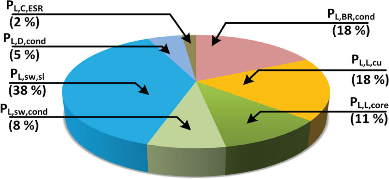
Figure 20.
Power loss distribution of the boost PFC converter. PFC, power factor correction.
Table 5.
Analytical loss models and derived current expressions for the PFC converter power-stage components.
| Components | Loss model | Analytical expression | Derived current expressions used for loss calculation |
|---|---|---|---|
| Bridge rectifier | Conduction loss, PL,BR,cond | ||
| Inductor | Copper loss, PL,L,cu | ||
| Core loss, PL,L,core | |||
| Switch (MOSFET) | Conduction loss, PL,sw,cond | ||
| Switching loss, PL,sw,sl | |||
| Diode | Conduction loss, PL,D,cond | ||
| Capacitor | ESR, PL,C,ESR |
[i] ESR, equivalent series resistance; fs, Switching frequency; IC,avg, Average capacitor current; IC,rms, RMS capacitor current; ID,avg, Average diode current; ID,rms, RMS diode current; Iin,avg, Average input current; Iin,rms, RMS input current; IL,avg, Average inductor current; IL,rms, RMS inductor current; IO, Output current; Isw,avg, Average switch current; Isw,rms, RMS switch current; PFC, power factor correction; Pv, Volumetric core loss density; rd, diode dynamic resistance; RDS(on), MOSFET’s on-resistance; RESR, ESR of capacitor; tf, Fall time; tr, Rise time; Vc, Core volume; VF, Diode forward voltage drop; Vin,pk, Peak input voltage; VO, Output voltage.
The converter efficiency is experimentally evaluated under six loading conditions spanning approximately 60%–120% of the rated power. The input and output voltages, currents, and PFs were measured under resistive loading, from which the input power, output power, and efficiency were computed. As shown in Figure 21, measured efficiency remained above 90% across the entire tested range, with a peak of 93% recorded at 936 W, and a near-unity PF (>0.999) maintained throughout. A polynomial curve fitted to the measured loss data, interpolated to the rated 900 W operating point, yielded an efficiency of 92.7%. The resulting 16 W difference, corresponding to a difference of 1.6 percentage points between the analytical and measured efficiencies, is consistent with system-level losses outside the scope of the five-component model, including gate-drive and auxiliary-supply consumption, electromagnetic interference (EMI) filter losses, current-sense resistor dissipation, PCB trace and connector resistance, and boost-diode reverse-recovery loss.
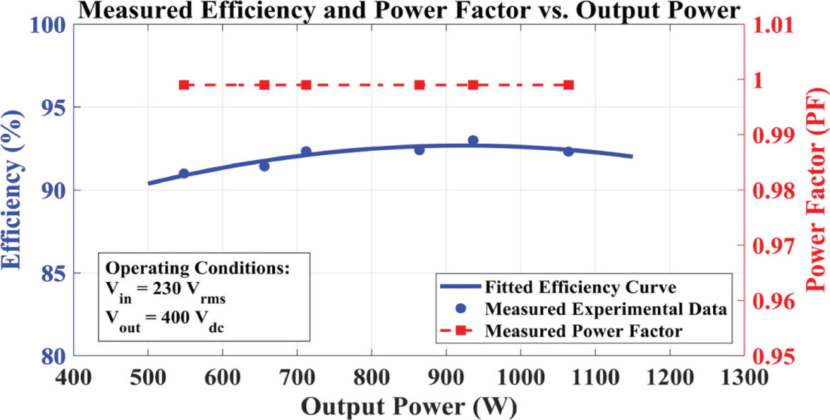
Figure 21.
Efficiency profile and PF performance of the proposed 900 W boost PFC prototype operating at a nominal input of 230Vrms. PF, power factor; PFC, power factor correction.
The experimental results validated the proposed control methodology, demonstrating a fast and stable voltage response with minimal overshoot, excellent load and line regulation, and consistent output stability. The system achieves a low THD, ensuring compliance with power quality standards, while effective PFC operation maintains a high PF and minimises input-current distortion. In addition, the controller exhibited robust dynamic performance and ensured stable DC-link voltage regulation. These findings confirm that the designed control strategy provides reliable and stable operation, making it well suited for ESP-based applications requiring HV, medium-power supplies.
7. Conclusion
This paper presents the design, modelling, and control of a front-end boost PFC converter for a HV supply intended for DBD-based ESP–NTP air purification systems. The proposed system operates under highly non-linear and time-varying loading conditions introduced by plasma inception dynamics in the DBD reactor. These non-linear characteristics impose strict constraints on the control bandwidth and system stability. To address these challenges, a FDM framework is developed to decouple fast inner current-loop dynamics from slow outer voltage-loop energy dynamics. A CCT model is introduced for the outer loop based on the average power behaviour of the PFC stage, enabling systematic controller design without reliance on conventional small-signal derivations. In addition, a GART method is proposed for DC-link capacitor selection by aligning plant resonance with grid frequency, thereby enabling low-distortion current shaping using a simple PI controller. A novel and generalised PI controller design procedure is also presented, eliminating the need for detailed small-signal derivations or iterative frequency-domain tuning for the PFC boost converter. Experimental validation of a 900 W single-phase prototype confirms a high PF, low THD, and robust DC bus regulation under dynamic operating conditions. The proposed methodology provides a framework for designing boost PFC stages in HV plasma systems, prioritising simplicity, robustness, and grid power quality compliance. FDM, along with GART, improves modelling accuracy and streamlines controller design by assigning appropriate frequency-domain models to control loops, with minimal distortion and low implementation complexity. Future work will extend this approach to other PFC topologies and develop adaptive control algorithms for enhanced robustness.