Figure 1
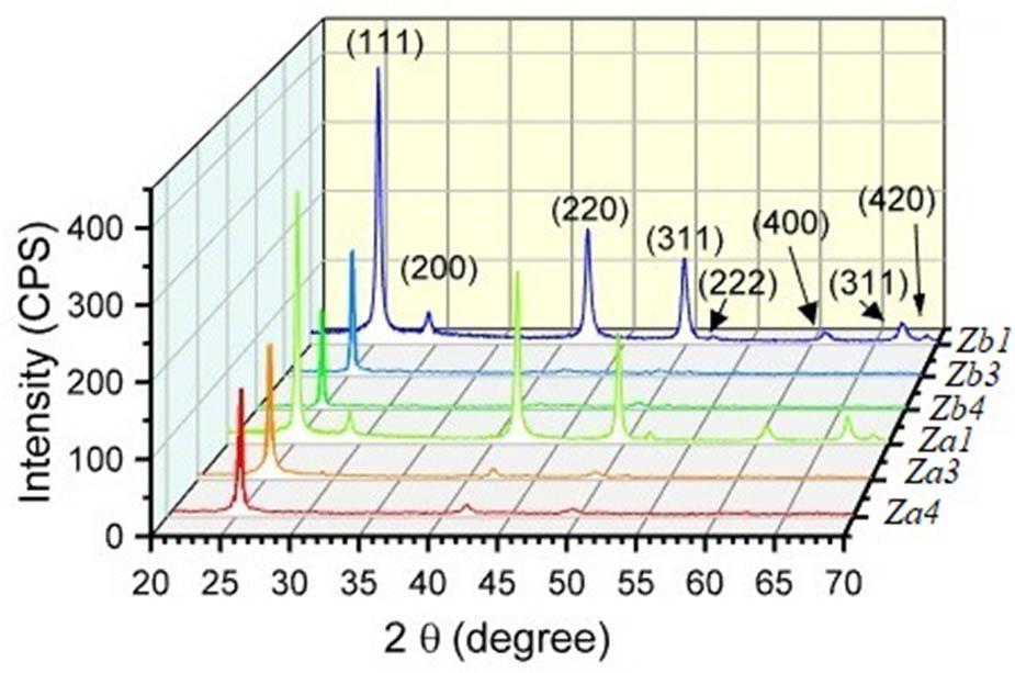
Figure 2
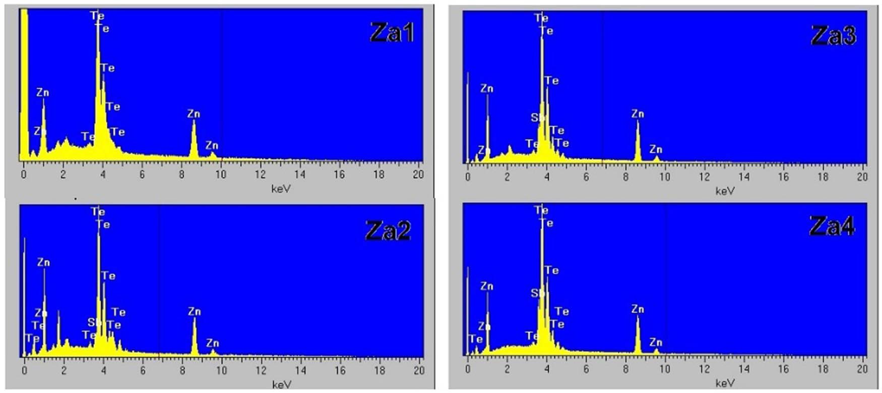
Figure 3
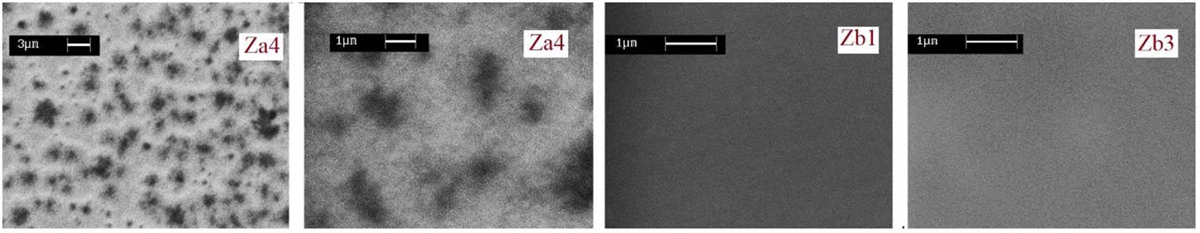
Figure 4
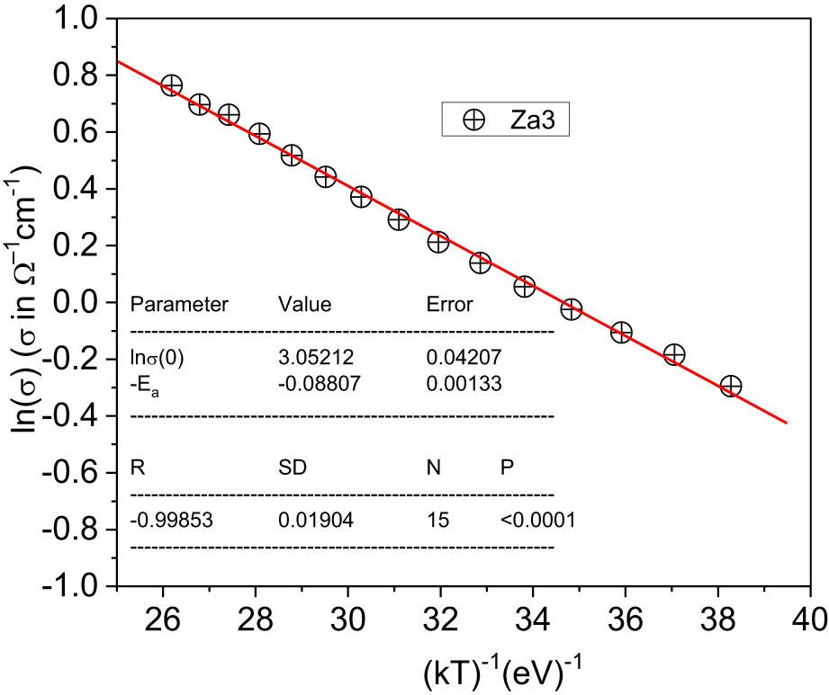
Figure 5
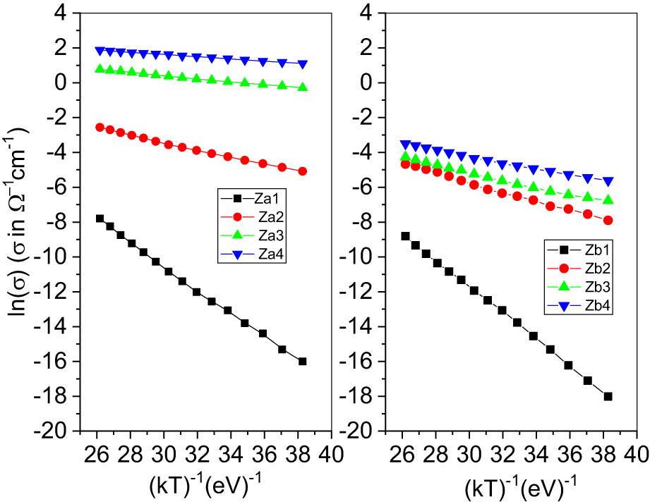
Figure 6
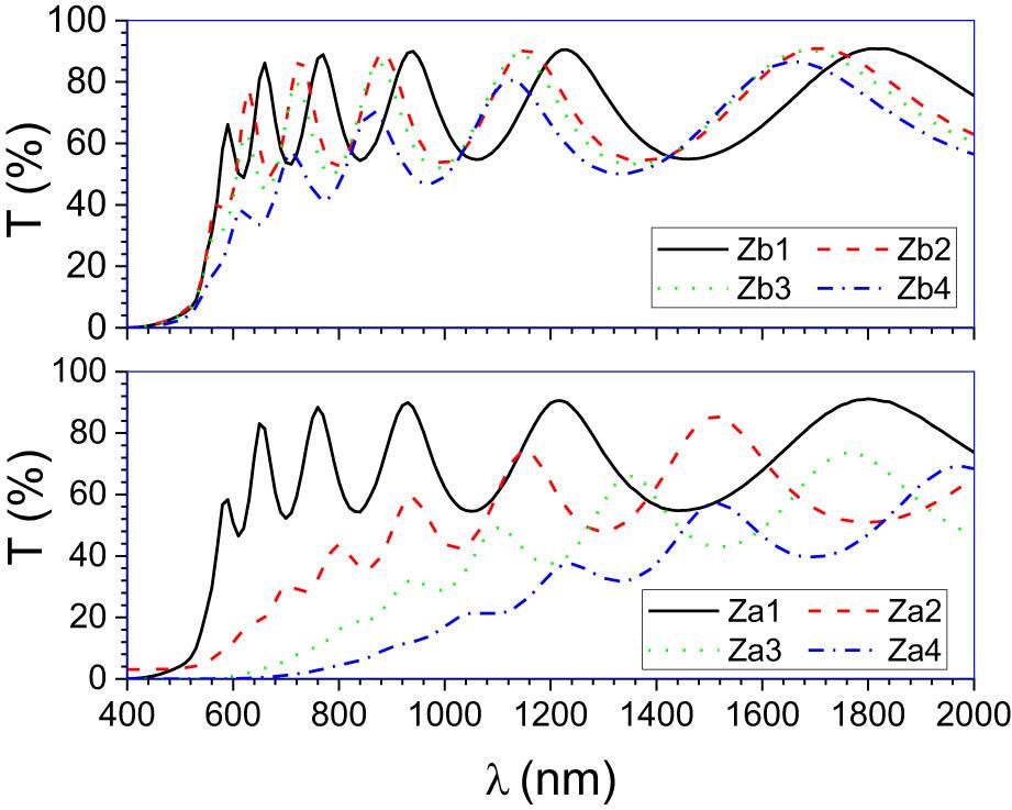
Figure 7
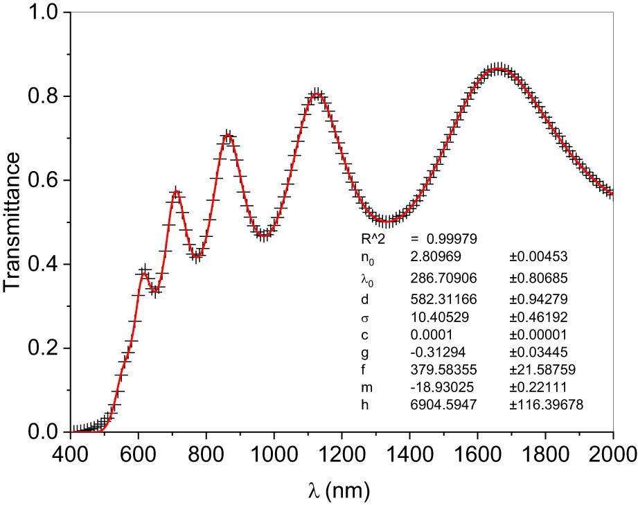
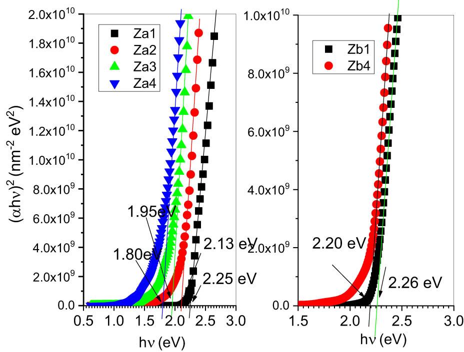
Figure 8
EDX and conductivity results_
| Film number | Zn ratio element % (±2%) | Te ratio element % (±2%) | Sb ratio element % (±2%) | Resistivity at 30°C (Ω-cm) | Conductivity activation energy (eV) |
|---|---|---|---|---|---|
| Za1 | 50.44 | 49.56 | — | 8.93 × 10⁶ | 0.68 |
| Za2 | 50.33 | 47.27 | 2.44 | 1.62 × 10² | 0.21 |
| Za3 | 49.54 | 44.28 | 8.18 | 1.34 × 101 | 0.09 |
| Za4 | 49.28 | 37.76 | 12.96 | 3.30 × 10⁻¹ | 0.06 |
| Zb1 | 50.14 | 49.86 | — | 6.72 × 10⁷ | 0.76 |
| Zb2 | 50.13 | 49.87 | — | 2.71 × 10³ | 0.27 |
| Zb3 | 50.16 | 49.84 | — | 8.70 × 10² | 0.21 |
| Zb4 | 50.10 | 48.49 | 1. 41 | 2.72 × 10² | 0.18 |
Results of the calculated optical parameters_
| Film number | Thickness (nm) | Root mean square roughness (nm) |
| Energy gap (eV) | |
|---|---|---|---|---|---|
| n o | λ o (nm) | ||||
| Za1 | 653 ± 3 | 12.3 ± 0.7 | 2.72 ± 0.01 | 292.5 ± 1.1 | 2.25 ± 0.005 |
| Za2 | 756 ± 1 | 09.9 ± 0.5 | 2.94 ± 0.01 | 299.7 ± 0.7 | 2.13 ± 0.005 |
| Za3 | 876 ± 3 | 16.0 ± 0.7 | 2.97 ± 0.01 | 348 ± 1.5 | 1.95 ± 0.005 |
| Za4 | 954 ± 4 | 18.2 ± 1.0 | 3.06 ± 0.02 | 363 ± 2.5 | 1.80 ± 0.005 |
| Zb1 | 660 ± 3 | 12.6 ± 0.7 | 2.71 ± 0.01 | 294.8 ± 1.0 | 2.26 ± 0.005 |
| Zb2 | 616 ± 2 | 9.7 ± 0.8 | 2.72 ± 0.01 | 298.5 ± 1.0 | 2.25 ± 0.005 |
| Zb3 | 601 ± 2 | 10.3 ± 0.6 | 2.76 ± 0.01 | 295.9 ± 0.9 | 2.22 ± 0.005 |
| Zb4 | 582 ± 1 | 10.4 ± 0.5 | 2.81 ± 0.01 | 286.7 ± 0.8 | 2.20 ± 0.005 |
Deposition parameters_
| Film number | Substrate temp. (°C) | Sb source temp. (°C) | Zn source temp. (°C) | Te source temp. (°C) | Sb evaporation rate (nm/s) |
|---|---|---|---|---|---|
| Za1 | 250 | — | 540 | 480 | — |
| Za2 | 250 | 560 | 540 | 480 | 1.1 |
| Za3 | 250 | 600 | 540 | 480 | 2.9 |
| Za4 | 250 | 640 | 540 | 480 | 5.2 |
| Zb1 | 350 | — | 540 | 480 | |
| Zb2 | 350 | 560 | 540 | 480 | 1.1 |
| Zb3 | 350 | 600 | 540 | 480 | 2.9 |
| Zb4 | 350 | 640 | 540 | 480 | 5.2 |