Tungstates, represented as MWO4 (where M is a metallic ion), are ternary oxide compounds containing the oxyanion of tungsten,
CdWO4 thin films can be synthesized using various techniques. Ziluei et al. have reported the preparation of CdWO4 films via spin-coating, using a suspension of CdWO4 in ethanol. These films exhibited photoluminescence (PL) when exposed to α-particles [3]. Another research group synthesized CdWO4 films through high-pressure sintering, observing a correlation between band gaps and PL properties [4].
The influence of temperature on hydrothermal synthesis, i.e. a solution-based synthesis at elevated temperatures has also been investigated. It was found that tungstates synthesized at higher temperatures without additional thermal treatment exhibit enhanced photocatalytic properties [5]. Recent studies have reported on CdWO4 thin films deposited via radiofrequency (RF) magnetron sputtering. RF sputtering has also been used to deposit composite CaWO4/CdWO4 films on SiO₂/Si substrates, using tungstate targets in an oxygen atmosphere. Films deposited at room temperature were found to be amorphous [6].
The primary challenges in synthesizing tungstate thin films include the deposition rate, the inherent insolubility of transition metal tungstates in water, and the absence of complexing agents. Additionally, nucleation and film quality are hindered by the high density of CdWO4 particles. The structural and optical properties of tungstates of type MWO4 (where M = Ni, Ba, or Bi) have been extensively studied. Research has shown that the PL of these compounds is highly dependent on their morphology [7]. For more complex systems, such as (1–x)CaWO4 xCdWO4, studies have demonstrated that the luminescence intensity is influenced by the crystal structure. Specifically, the monoclinic phase exhibits higher luminescence intensity than the tetragonal phase. Additionally, the luminescence intensity increases significantly with a higher Cd concentration [8,9]. Shang et al. [10] investigated the PL properties of CdWO4 films doped with Li⁺, Bi3⁺, and B3⁺, synthesized using the sol–gel method. These films exhibited notable PL. Similarly, PL has been observed in CdWO4 doped with 0.1% Mo [11].
Chemical bath deposition (CBD) offers significant advantages due to its speed, efficiency, and ability to control the chemical composition of the film with ease. A common challenge with this method is film adhesion to the substrate; however, in this case, the presence of peroxide and the complex decomposition mechanism of the tungstate precursor effectively mitigated this issue. Sol–gel techniques enable easy coating of large surfaces but require careful thermal treatment, as residual organic compounds such as citric acid, glycerol, and glycol can lead to further chemical changes on the films during annealing. RF sputtering, while capable of producing highly uniform and high-quality films, is limited by slow deposition rates and the need for substantial capital investment in high-vacuum systems, magnetrons, and power sources.
The electrochromic properties of tungsten(
To synthesize CdWO4, the following precursor solution was prepared: 5 g of tungstic acid (H2WO4, Thermo Scientific Chemicals, 99+%) was dissolved in 40 mL of hot 30% hydrogen peroxide (H2O2, ROTIPURAN® 30%, Carl Roth) under continuous stirring for 3 h until complete dissolution, yielding a transparent solution. The solution was then heated to 80°C, and with constant stirring, a stoichiometric amount of 6.15 g of cadmium nitrate (Cd(NO3)2·4H2O, 99+%, Thermo Scientific Chemicals) was added. Initially, a milky white suspension formed, which gradually became translucent upon vigorous stirring. The solution volume was adjusted to 50 mL with deionized (DI) water, resulting in a final pH of 4. The prepared solution was stable and could be stored for later use. All chemicals used in this study were of reagent-grade.
CdWO4 films were deposited onto microscope glass substrates, which were pre-cleaned using concentrated chromic/sulfuric acid, followed by rinsing with deionized water and isopropanol. Before deposition, the clean, dry glass substrates were stored in a desiccator containing silica gel.
For thin film deposition, the CdWO4 precursor solution was placed in a beaker on a magnetic stirrer, and the glass substrates were positioned vertically. The solution was heated to 80–90°C, and deposition was carried out for 20 min. For electrochromic measurements, CdWO4 films were deposited on transparent indium tin oxide (ITO) conductive glass substrates with a nominal resistivity of 10 Ω/sq.
The reactions leading to the formation of CdWO4 were as follows:
The Cd-complex instantly started decomposing to CdWO4:
These reactions led to the precipitation of CdWO4 onto the glass substrates. The formation of CdWO4 films from the Cd-complex continued in the drying chamber, where the films were heated to 90°C for 2 h. After spontaneous cooling to room temperature, the films underwent thermal treatment in a muffle furnace with a gradual temperature increase from room temperature to 600°C over 3 h. The films were then maintained at 600°C for 1 h before being allowed to cool naturally to room temperature overnight. The deposited films exhibit a maximum transmittance variation of ±5% T units from batch to batch, as measured using a UV-vis spectrophotometer. The transmittance spectra were also stable over time.
CdWO4 films were morphologically characterized using a TESCAN Vega 3 scanning electron microscope equipped with an Oxford Instruments energy-dispersive X-ray (EDX) detector for elemental analysis. Before analysis, the samples were mounted on a stage using carbon tape and coated with a 5–10 nm gold layer using a direct current (DC) sputtering machine for 1 min at a constant sputtering rate.
X-ray diffraction (XRD) measurements were performed using a Shimadzu LabX XRD-6100 diffractometer, scanning in the 2θ range from 10° to 80°. The crystallite size was assessed by evaluating the full width at half-maximum (FWHM, β) of the most intense diffraction peaks (−111) and (111) using a peak-fitting procedure with a Gaussian function. The crystallite size (D) was calculated using the modified Debye–Scherrer equation as follows:
UV-vis transmittance spectra were recorded using a BioBase 1800 UV-vis spectrophotometer in the range of 380–1,080 nm, with a resolution of 0.5 nm. A blank microscope slide was used for baseline correction.
Fourier transform infrared (FTIR) spectra were obtained using a Shimadzu IRAffinity-1 FTIR interferometer with a Specac high-temperature ATR cell (model Golden Gate) equipped with a diamond window. The spectral resolution was set to 4 cm⁻1, with 32 scans per run.
Non-polarized Raman spectra were recorded using a Horiba Jobin Yvon LabRam 300 Infinity micro-Raman spectrometer with a 632.8 nm He–Ne laser for excitation. The spectral resolution was set to 4 cm⁻1, with 16 scans per spectrum. Raman spectra were collected from films deposited on glass substrates, while FTIR spectra recorded from scratched powder samples obtained from the film surfaces.
PL measurements were conducted using a custom-built setup featuring a 100 W/2 HBO mercury vapour lamp for excitation and a UV-vis modular spectrometer (USB4000, Ocean Optics). The full excitation spectrum from the mercury lamp was directed onto the thin films to induce PL, which was collected using fibre-optic waveguides. The collection angle was manually adjusted for the maximum intensity. The emission/reflectance spectra were recorded over a range of 380–1,080 nm, with a resolution of 0.2 nm and a spectral integration time of 200 ms.
Simple electrochromic tests were performed using a Siglent SDG1032X function/arbitrary waveform generator as a DC source. A two-electrode electrochemical cell was assembled, with a platinum (Pt) electrode as the anode, a CdWO4-coated FTO substrate as the cathode, and 0.1 M citric acid (99+%, Thermo Scientific Chemicals) aqueous solution as the electrolyte. The cathode was biased with +5 V DC against the Pt anode to achieve the electrochromic colouration. The coloured film was removed from the solution, washed, and quickly dried with dry nitrogen. The film transmittance spectra of the film in its coloured and bleached states were then measured using a vis-NIR spectrophotometer. Before each measurement, the spectrometer blank probe was recorded on FTO-coated glass.
All morphological, elemental, structural, optical, and spectroscopic characterization studies (including PL) were conducted at room temperature.
The deposited thin films appeared translucent white and exhibited strong adhesion to the substrate. The scanning electron microscopy (SEM) image in Figure 1 reveals the surface morphology of the annealed CdWO4 films, showing multiple surface defects, including cracks and craters. These defects likely result from the release of oxygen due to the thermal degradation of the cadmium peroxotungstate complex, as described in the chemical reactions in the previous section. The inset micrograph displays a densely packed grain structure with poorly defined grain shapes and boundaries. Elemental analysis from the EDX spectra of the films annealed at 600°C is presented in Table 1.
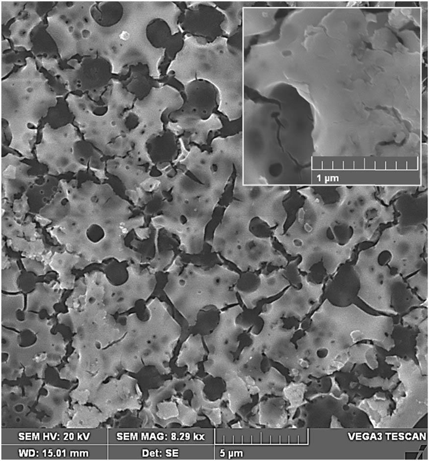
SEM micrograph of the annealed CdWO4 film. Inset is an image with greater resolution.
EDX quantitative elemental analysis of the annealed film at 600°C.
| Spectral line | At% experimental/EDX | At% theoretical for CdWO4 |
|---|---|---|
| O K | 89.1 | 66.7 |
| Cd L | 4.2 | 16.7 |
| W M | 6.7 | 16.7 |
Apart from the expected surplus of oxygen content due to surface contamination from air, the EDX analysis results presented in Table 1 reveals that the compound is nonstoichiometric. Specifically, the Cd/W ratio is approximately 2:3 instead of the expected 1:1, indicating an excess of tungsten in the composition. Similar nonstoichiometric films rich in tungsten have also been reported by other researchers [3] using the sol–gel technique. There may be several reasons for the non-stoichiometry of the compound. Previous authors [14,15] have reported the high volatility of Cd and its compounds during thermal treatment, as well as heat-induced diffusion into the film.
Figure 2(a) presents the transmission spectra recorded in the 380–1,180 nm range. Both as-prepared and annealed (600°C) films exhibit high transparency in the visible region. Notably, thermal treatment at 600°C slightly increased the transparency in the red region. Figure 2(b) and (c) illustrate the evaluation of the band gap using the Tauc plot [16], assuming a direct transition. The estimated band gap values for the as-prepared (unannealed) film and the annealed (600°C) film are 2.71 eV (Figure 2(b)) and 2.62 eV (Figure 2(c)), respectively. These values are consistent with those reported for single crystals of CdWO4 [17]. The observed narrowing of the band gap after thermal treatment at 600°C suggests a red shift, likely due to improved crystallization, as further confirmed by the XRD and Raman results presented below. In addition, the observed gap narrowing could also be attributed to the excess of tungsten (W-rich composition), which may introduce donor-like defect states in the band gap. Annealing could cause these defect states to merge with the conduction or valence band, leading to an apparent narrowing of the band gap.
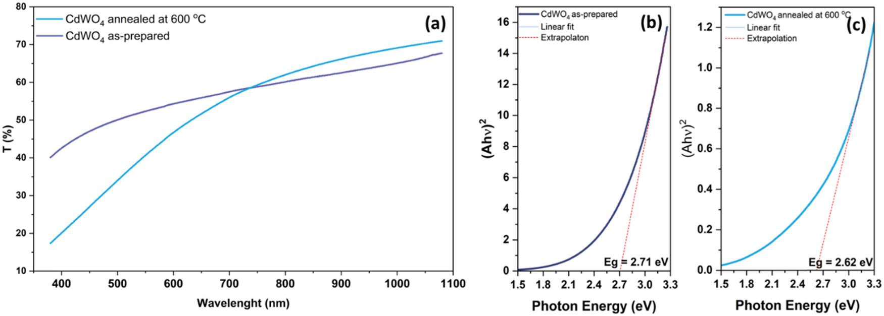
(a) Transmission spectra of CdWO4 films; Tauc plot of (b) as-prepared and (c) annealed at 600°C CdWO4 films.
Although extensive literature exists on various transition metal tungstates, the assignment of stretching and bending modes has primarily been conducted for bulk crystals, single crystals, and nanoparticles [18–20]. However, studies dedicated to the interpretation of the spectra of these thin films remain limited. According to the group theory, the tungstate group reveals a space group symmetry of
The FTIR spectra in Figure 3 suggest the presence of two vibration modes: a strong symmetric W–O stretching (ν 1) at 887 and 881 cm−1 and an asymmetric W–O stretching mode (ν ₃) at 797 and 802 cm−1 in both the as-prepared and annealed films, respectively. Also, an intense band from the valence OH̶ vibration of water molecules (in the 3,800–3,000 cm−1 region) is evident in the as-deposited film only. These transmittance minima are also extracted and assigned to the respective vibrations in Table 2. These spectra strongly suggest that CdWO4 films improved their crystallinity upon thermal treatment at 600°C.
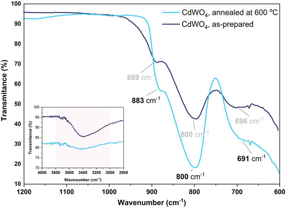
ATR-FTIR spectra of CdWO4 films, as-prepared and annealed at 600°C.
IR vibration modes of the unannealed and annealed CdWO4 films.
| IR, vibration mode –as-prepared CdWO4 film (cm−1) | IR, vibration mode –CdWO4 film annealed at 600°C (cm−1) | Reference [23] (cm−1) |
|---|---|---|
| 887, ν 1 | 881, ν 1 | 885, 835, and 700 |
| 797, ν 3 | 802, ν 3 | 796 |
| 696, (weak), ν 1 | 687, (shoulder), ν 1 | 795 |
The identified Raman shifts in Figure 4 were found to originate from CdWO4, with all four vibration modes present (ν 1–ν 4). The assigned Raman shifts are listed in Table 3 along with literature data for comparison. The presence of lattice vibration modes in the Raman spectra provided strong evidence of the crystalline nature of the films. This finding aligns well with previously reported data on CdWO4 [4].
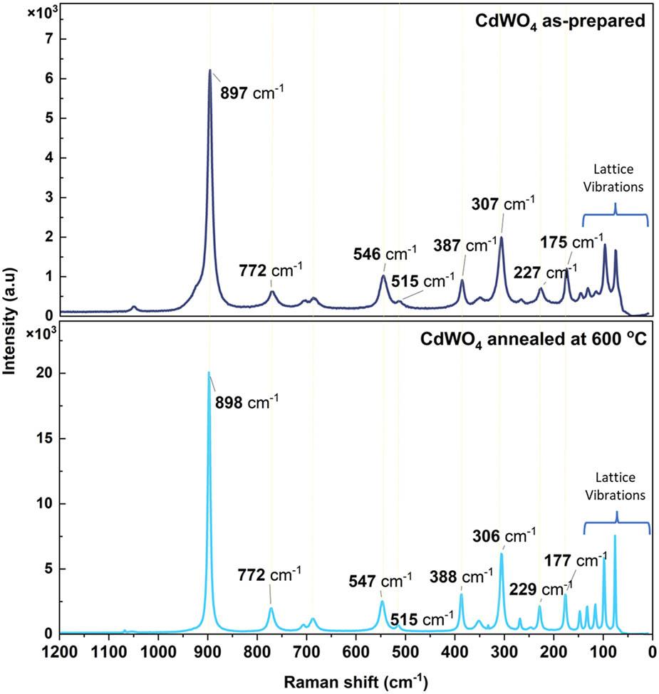
Raman spectra of CdWO4 thin films, as-prepared and annealed at 600°C.
Raman vibrations of the unannealed and annealed CdWO4 films.
| Raman shift, vibration mode – as-prepared CdWO4 film (cm−1) | Raman shift, vibration mode – CdWO4 film annealed at 600°C (cm−1) | Reference [22] (cm−1) |
|---|---|---|
| 898, ν 1 | 897, ν 1 | 900 |
| 546, 387, and 307, ν 2 | 547, 388, and 306, ν 2 | 550, 390, and 308 |
| 772, ν 3 | 772, ν 3 | 776 |
| 515, ν 4 | 515, ν 4 | 522 |
| 145, 132, 114, 98, and 75, lattice vibr. | 147, 133, 116, 97, and 77, lattice vibr. |
The X-ray diffractograms of unannealed and annealed at 600°C films, along with the corresponding JCPDS 14-0676 reference pattern of a monoclinic phase CdWO4, are presented in Figure 5(a). The calculated cell parameters were found to be a = 0.522 nm, b = 0.588 nm, c = 0.508 nm, and β = 91.8° for the as-prepared sample and a = 0.503 nm, b = 0.589 nm, c = 0.525 nm, and β = 95.8° for the annealed sample. These results are consistent with previously reported lattice parameters for CdWO4 synthesized using the sol–gel method, further confirming the monoclinic phase structure [25,26]. From the XRD patterns, it is evident that thermal treatment enhanced the crystallinity, as indicated by the increased intensity and sharper diffraction peaks. The average crystallite size, calculated from the (111) peak [27] (Figure 5(b)), confirms crystallite growth due to annealing at 600°C, increasing their diameter (D) of a spherical shape approximation from 9.8 nm (as-prepared) to 23.6 nm (annealed). Additionally, the XRD patterns reveal the presence of secondary phases (CdO and WO₃), which became more detectable in the annealed sample, suggesting partial decomposition or phase segregation during thermal treatment.
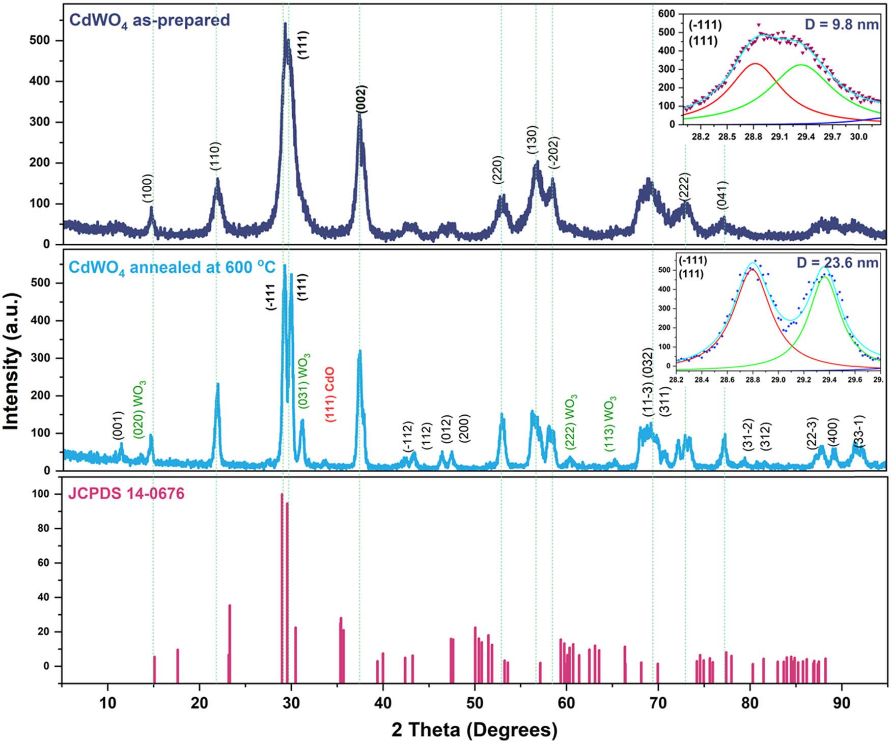
X-ray diffractogram of CdWO4 thin films: as-prepared and annealed at 600°C, along with the JCPDS 14-0676 standard reference file. Multi-peak deconvolution of diffraction maxima (−1, 1, 1) and (1, 1, 1) to evaluate the FWHM of (1, 1, 1) at a 2θ angle 29.35°, to calculate the crystallite size (D) (insets).
Furthermore, the observed band gap reduction could be attributed to crystallite enlargement, which is an expected outcome. It is well known that the crystallite size (D) influences the band gap (E g). Specifically, smaller crystallites often exhibit quantum confinement effects, resulting in a larger band gap, whereas films with larger crystallites tend to approach the bulk band gap value [28].
The intrinsic PL of CdWO4 films, excited with a discrete excitation wavelength of 254 nm, is presented in Figure 6. As evident from the figure, the film annealed at 600°C exhibited approximately 50% higher luminescence intensity than the as-prepared film, aligning with the findings reported by other authors [26]. The broad PL peak at 500 nm (∼2.48 eV), with an FWHM of ∼100 nm, suggested that the radiative recombination process involves multiple states, strong phonon interactions, or structural inhomogeneities, contributing to line broadening. Possible factors responsible for this broadening include the formation of multiple shallow donor energy levels within the band gap due to oxygen vacancies or tungsten-related defects, consistent with the W-rich composition observed in EDX analysis, and the charge transfer between oxygen and tungsten ions (O2– → W6+), a process known to contribute to exciton dynamics and broaden luminescence bands in tungstate-based materials like CdWO4 [29]. The 2.48 eV emission may also be associated with the radiative recombination mechanism of WO₃, an indirect semiconductor with a band gap of ∼2.5 eV [30], detected as a secondary phase in the XRD pattern. Rzevskaya et al. [11] reported that the maximum emission band in their study, observed at 2.46 eV (∼500 nm), corresponds to the radiative decay of an exciton self-trapped at
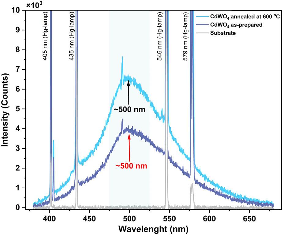
PL along with the reflectance spectrum of CdWO4 thin films (excitation: 254 nm with a Hg lamp). The grey spectrum was recorded from a blank substrate (glass slide) under Hg lamp illumination.
Similar luminescence spectra were reported by Shang et al. [26] with a maximum appearing at around 500 nm and by Eranjaneya and Chandrappa with a maximum at 473 nm [25] for nanoparticles synthesized by the combustion method.
Bearing in mind that the CdWO4 films in this work are rich in W (with reference to our present EDX results) and contain a WO3 secondary phase (our XRD results), it was assumed that they may exhibit electrochromic behaviour. To test this assumption, the CdWO4 films were deposited onto conductive transparent electrodes of indium-doped tin oxide (ITO) and annealed at 600°C. The provisional electrochromic cell was formed in a beaker using a Pt electrode as the anode and the CdWO4/FTO film as the cathode in 0.1 M citric acid. When biased with +5 V, an electrochromic reaction occurred on the film, clearly displaying cathodic electrochromism. In other words, the CdWO4 films switched their colour from transparent to dark grey (Figure 7). The process was reversible. When the polarity was altered, the films turned back to being transparent. The transmittance spectra of coloured (excited) and as-is films in the visible light range show that in the vicinity of 550 nm (the peak output of sunlight irradiance), the change in the transparency of the films was ΔT = 55%.
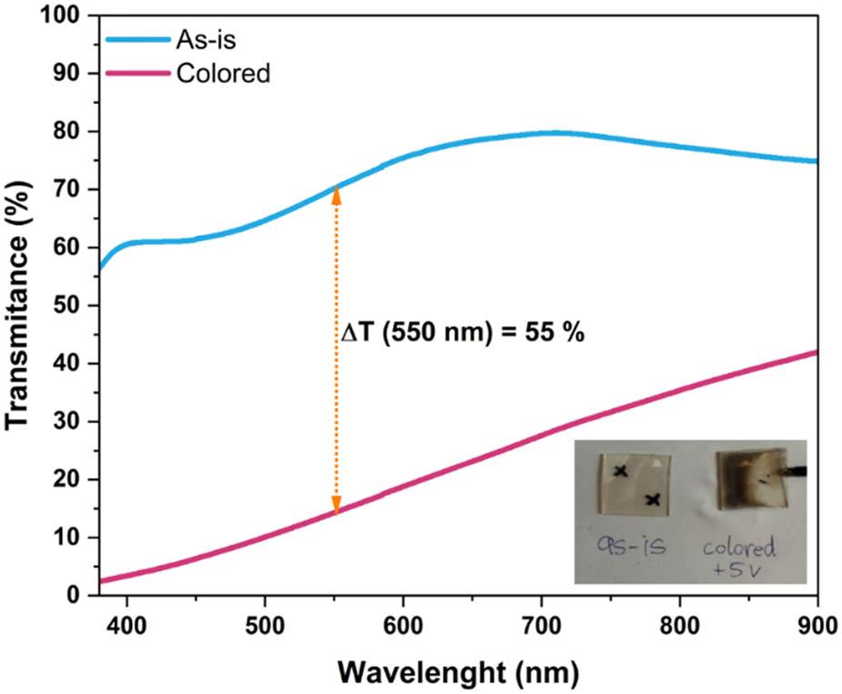
Transmission spectra of the as-is and coloured CdWO4 films.
CdWO4 thin films were successfully synthesized using a simple and cost-effective CBD method. XRD analysis confirmed the formation of monoclinic CdWO4, although secondary phases of WO₃ and CdO were also detected. The films were found to be W-rich with the Cd/W ratio of 2:3, despite the stoichiometric ratio in the precursor solution. Hence, in order to produce a stoichiometric or even Cd-rich compound, one should consider examination of the influence of Cd/W > 1 ratios in the precursor solution. Thermal treatment significantly improved the crystallinity and adhesion of the films, as evidenced by XRD, Raman, and FTIR results. XRD analysis revealed that the crystallite size increased from 9.8 to 23.6 nm upon annealing at 600°C. The films exhibited intrinsic PL under high-energy UV radiation, with a broad emission maximum at 500 nm. Notably, annealed CdWO4 films displayed considerably higher PL intensity compared to the as-prepared samples. Preliminary electrochromic tests indicated that CdWO4 films exhibit reversible cathodic electrochromic colouration. The electrochromic behaviour of CdWO4 films will be the subject of our future research. Further optimization of preparation parameters is necessary to enhance the PL performance for both UV and X-ray excitation sources by increasing the Cd content, making these films viable for photon detection applications.
This research was sponsored by the Western Balkans Mobility Scheme – A Policy Answers Pilot Programme as an integral part of the project Preparation and Characterization of Tungstates and Oxide Semiconductor Thin Films (MEWO-019). We kindly acknowledge and deeply thank Dr Tena Sijakova-Ivanova for recording the XRD patterns and Maja Ristova-Delietrev for performing the SEM/EDX measurements (both from the School of Geology at the University Goce Delcev Stip, North Macedonia). We also express our gratitude to Dr Miha Bukleski from the Chemistry Department at the Faculty of Natural Sciences and Mathematics, University Ss Cyril and Methodius, Skopje, for acquiring the Raman spectra for this study.
This research was sponsored by the Western Balkans Mobility Scheme – A Policy Answers Pilot Programme as an integral part of the project Preparation and Characterization of Tungstates and Oxide Semiconductor Thin Films (MEWO-019).
Conceptualization: Mimoza Ristova, Stefan Jovanovski. Methodology: Mimoza Ristova, Stefan Jovanovski. Investigation: Mimoza Ristova, Stefan Jovanovski. Data Curation: Mimoza Ristova, Stefan Jovanovski. Writing–Original Draft: Mimoza Ristova, Stefan Jovanovski. Writing–Review & Editing: Mimoza Ristova, Stefan Jovanovski.
Authors state no conflict of interest.
The data that support the findings of this study are available from the corresponding author upon reasonable request.