
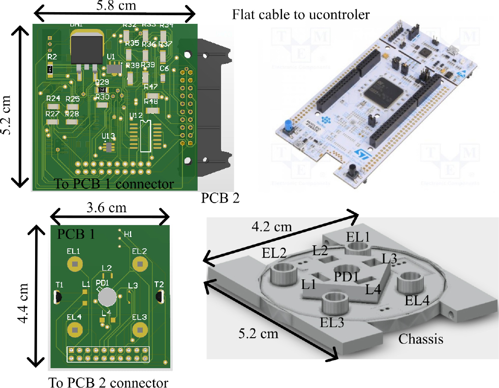
Figure 1:
System diagram for the current device under development.
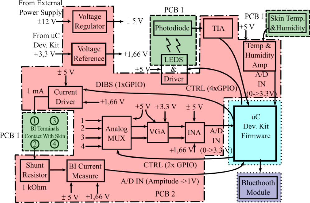
Figure 2:
System diagram for the current device under development.
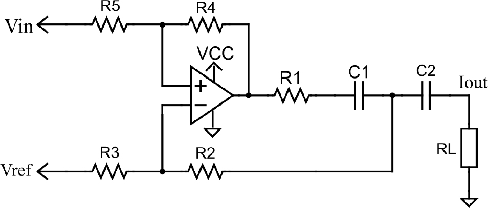
Figure 3:
Enhanced Howland Current source Schematic.
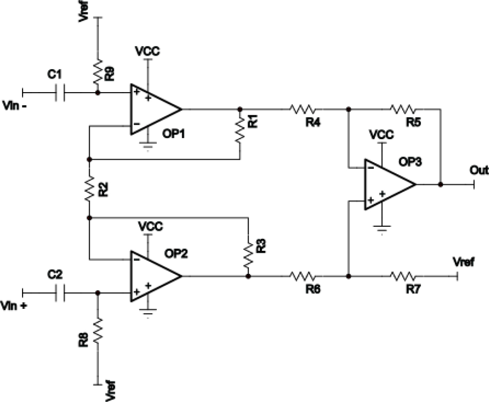
Figure 4:
Instrumentation Amplifier Schematic.
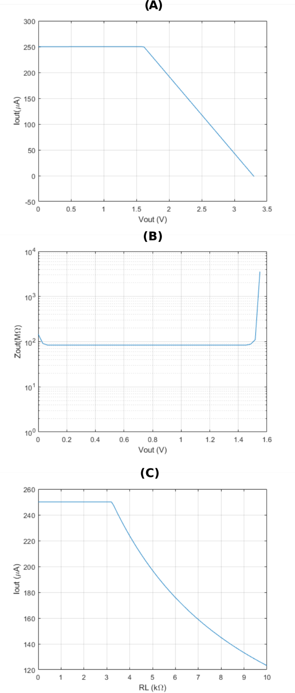
Figure 5:
DC simulation results for the low power supply design.
Table 1:
CC output current (in μA) considering temperature and voltage supply corners.
| Topology | Iout (0<T<100°C) | Iout (1.8<VCC<3.3V) |
|---|---|---|
| EHCS | 250.118 to 250.121 | 249.97 to 250.12 |
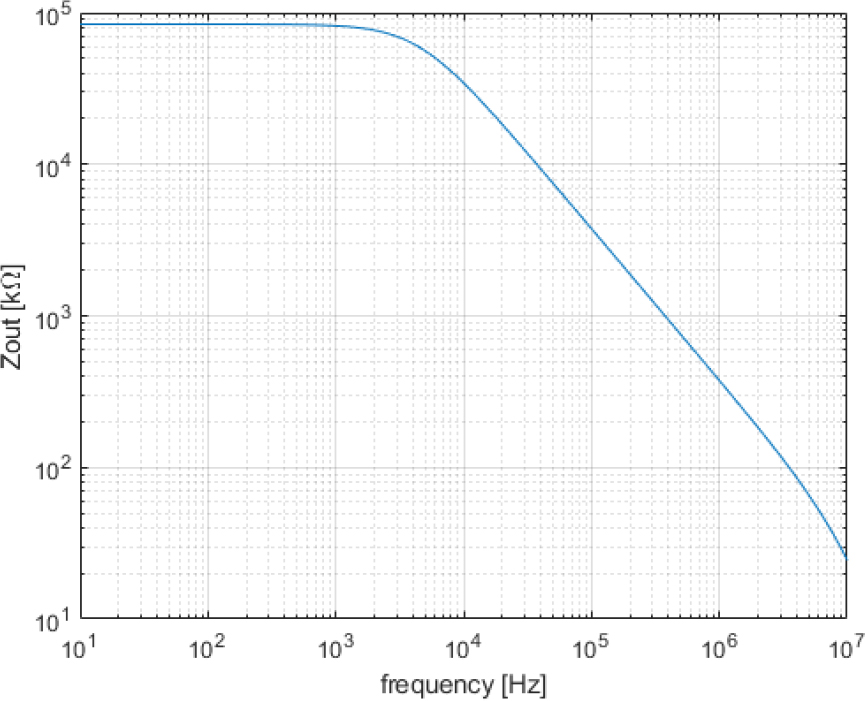
Figure 6:
Output impedance versus frequency in AC analysis.
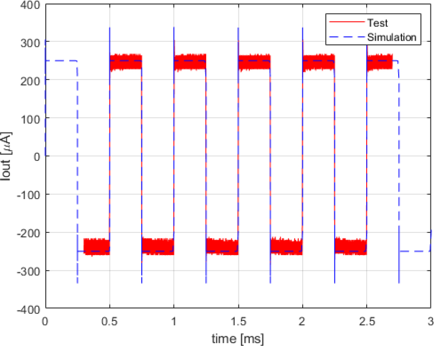
Figure 7:
Simulation vs test output current comparison for 2 : kHz rectangle wave.
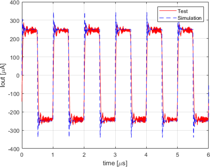
Figure 8:
Simulation vs test output current comparison for 1 MHz rectangle wave.
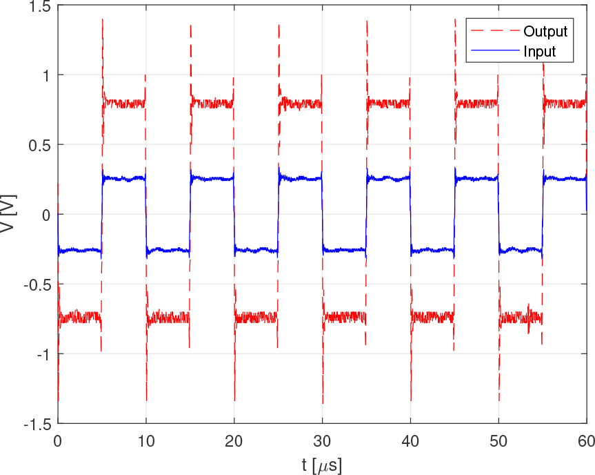
Figure 9:
Instrumentation amplifier test with a 1 KΩ impedance for a 100 kHz rectangle wave.
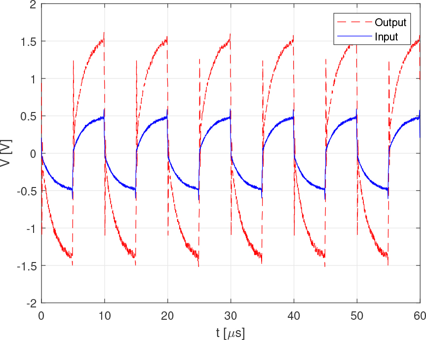
Figure 10:
Instrumentation amplifier test with a Cole impedance for a 100 kHz rectangle wave.
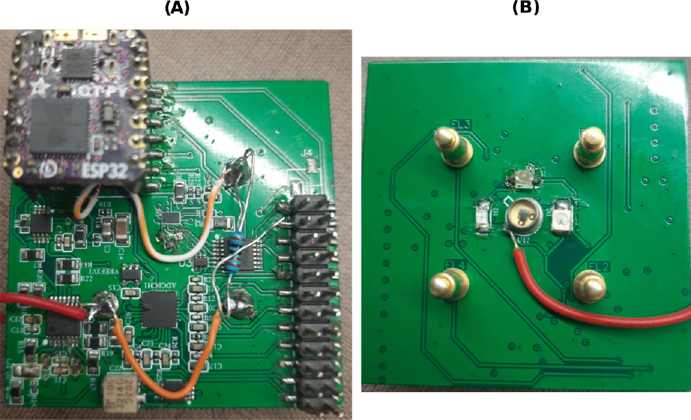
Figure 11:
Shrink prototype (A) top view and (B) bottom view.