
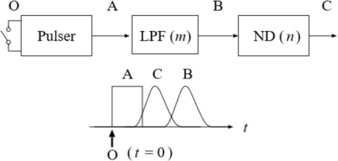
Figure 1.
Experimental schematic diagram of negative group delay and the pulse relationship on the time axis
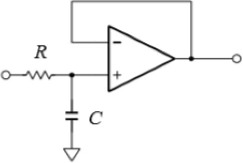
Figure 2.
A first-order RC circuits with positive group delay
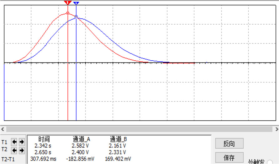
Figure 3.
Simulation effect of first-order RC circuits with positive group delay
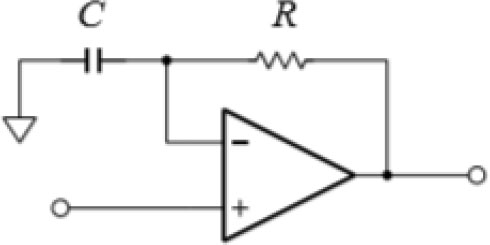
Figure 4.
A first-order RC circuits with negative group delay
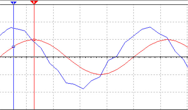
Figure 5.
Simulation effect of first-order RC circuits with negative group delay
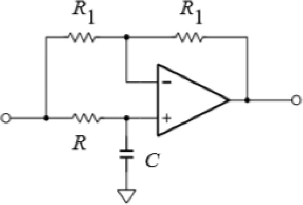
Figure 6.
A first-order filter for modulating the input pulse
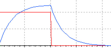
Figure 7.
Simulation results of first-order filter modulating rectangular pulse
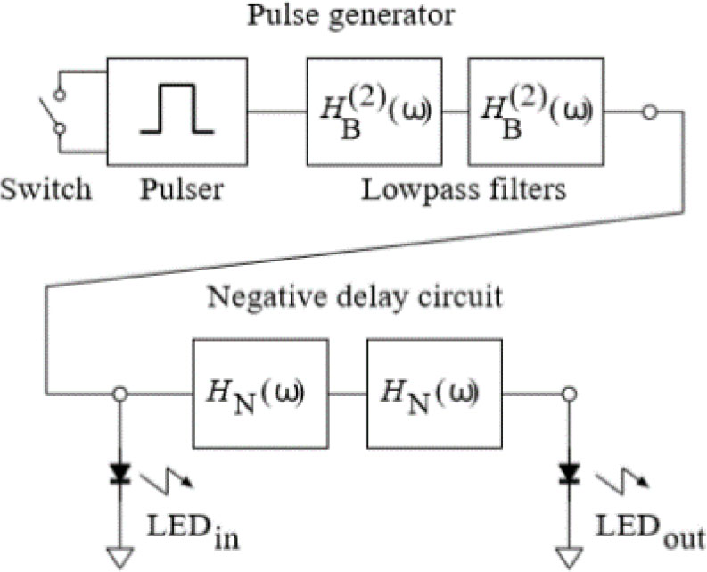
Figure 8.
The electronic circuit realizing the negative group delay phenomenon
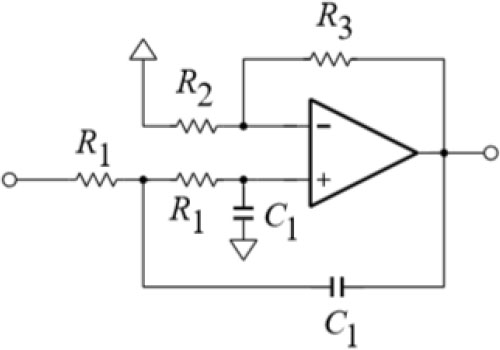
Figure 9.
Second-order Bessel filter
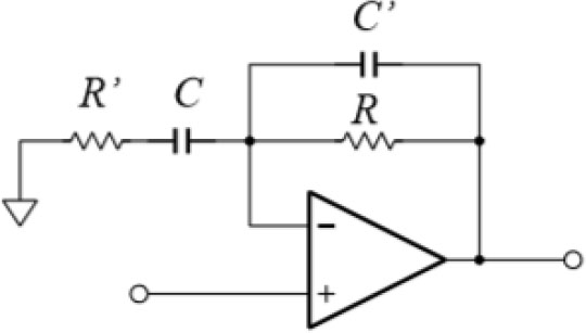
Figure 10.
Negative group delay electronic circuit
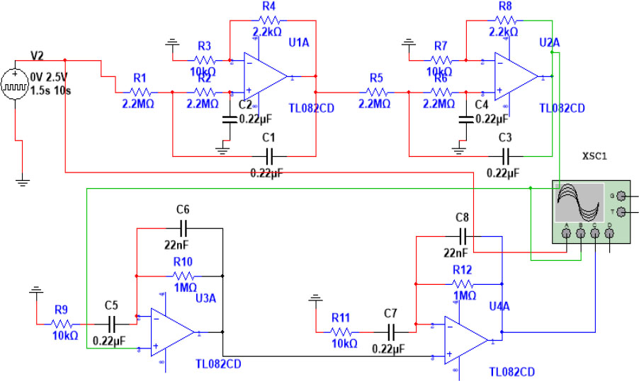
Figure 11.
Electronic route built in simulation software
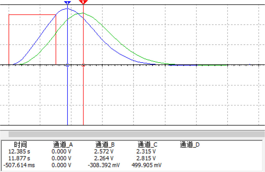
Figure 12.
Simulation results of negative group delay phenomenon
TABLE I.
Simulation results of adjusting the ratio of the number of bessel filters and negative group delay circuits
| BF | NGD | NDT/ms | IPP/V | OPP/V | AMP |
|---|---|---|---|---|---|
| 2 | 1 | 214 | 2.577 | 2.685 | 1.042 |
| 2 | 2 | 427 | 2.577 | 2.81 | 1.090 |
| 2 | 3 | 615 | 2.577 | 3.007 | 1.167 |
| 2 | 4 | 803 | 2.577 | 3.215 | 1.248 |
| 3 | 1 | 205 | 2.677 | 2.754 | 1.029 |
| 3 | 2 | 479 | 2.677 | 2.837 | 1.060 |
| 3 | 3 | 615 | 2.677 | 2.946 | 1.101 |
| 3 | 4 | 821 | 2.677 | 3.053 | 1.140 |
| 3 | 5 | 1027 | |||
| 3 | 6 | 1164 | |||
| 4 | 1 | 256 | 2.903 | 2.968 | 1.022 |
| 4 | 2 | 462 | 2.903 | 3.036 | 1.046 |
| 4 | 3 | 701 | 2.903 | 3.116 | 1.073 |
| 4 | 4 | 889 | 2.093 | 3.187 | 1.098 |
| 4 | 5 | 1068 | |||
| 4 | 6 | 1099 | |||
| 4 | 7 | 1294 | |||
| 5 | 1 | 205 | 3.229 | 3.288 | 1.018 |
| 5 | 2 | 462 | 3.229 | 3.351 | 1.038 |
| 5 | 3 | 752 | 3.229 | 3.432 | 1.063 |
| 5 | 4 | 906 | 3.229 | 3.48 | 1.078 |
| 5 | 5 | 1050 | |||
| 5 | 6 | 1205 | |||
| 5 | 7 | 1378 | |||
| 6 | 1 | 222 | 3.652 | 3.709 | 1.016 |
| 6 | 2 | 427 | 3.652 | 3.767 | 1.031 |
| 6 | 3 | 701 | 3.652 | 3.829 | 1.048 |
| 6 | 4 | 940 | 3.652 | 3.902 | 1.068 |
| 6 | 5 | 1022 | |||
| 6 | 6 | 1265 | |||
| 6 | 7 | 1425 | |||
| 7 | 1 | 239 | 4.179 | 4.236 | 1.014 |
| 7 | 2 | 444 | 4.179 | 4.295 | 1.028 |
| 7 | 3 | 718 | 4.179 | 4.358 | 1.043 |
| 7 | 4 | 889 | 4.179 | 4.46 | 1.067 |
| 7 | 5 | 933 | |||
| 7 | 6 | 1134 | |||
| 7 | 7 | 1283 | |||
| 8 | 1 | 205 | 4.827 | 4.886 | 1.012 |
| 8 | 2 | 444 | 4.827 | 4.946 | 1.027 |
| 8 | 3 | 684 | 4.827 | 5.008 | 1.037 |
| 8 | 4 | 855 | 4.827 | 5.064 | 1.049 |
| 8 | 5 | 1004 | |||
| 8 | 6 | 1199 | |||
| 8 | 7 | 1283 | |||
| 9 | 1 | 239 | 5.618 | 5.678 | 1.011 |
| 9 | 2 | 444 | 5.618 | 5.74 | 1.022 |
| 9 | 3 | 615 | 5.618 | 5.803 | 1.033 |
| 9 | 4 | 889 | 5.618 | 5.872 | 1.045 |
| 9 | 5 | 1060 | |||
| 9 | 6 | 1186 | |||
| 9 | 7 | 1345 | |||
| 10 | 1 | 251 | 6.503 | 6.565 | 1.010 |
| 10 | 2 | 474 | 6.503 | 6.63 | 1.020 |
| 10 | 3 | 669 | 6.503 | 6.697 | 1.030 |
| 10 | 4 | 865 | 6.503 | 6.762 | 1.040 |
| 10 | 5 | 1088 | |||
| 10 | 6 | 1199 | |||
| 10 | 7 | 1381 |
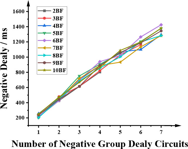
Figure 13.
The variation of delay time with the number of circuits under different Bessel filters numbers
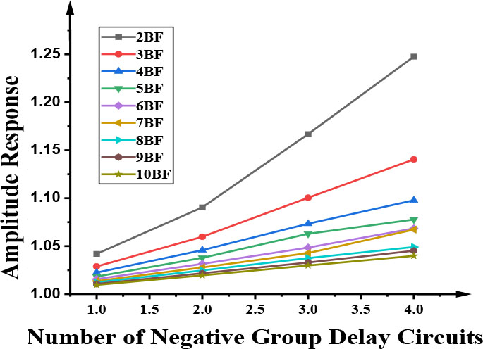
Figure 14.
Amplitude response varies with the number of circuits under different Bessel filters numbers
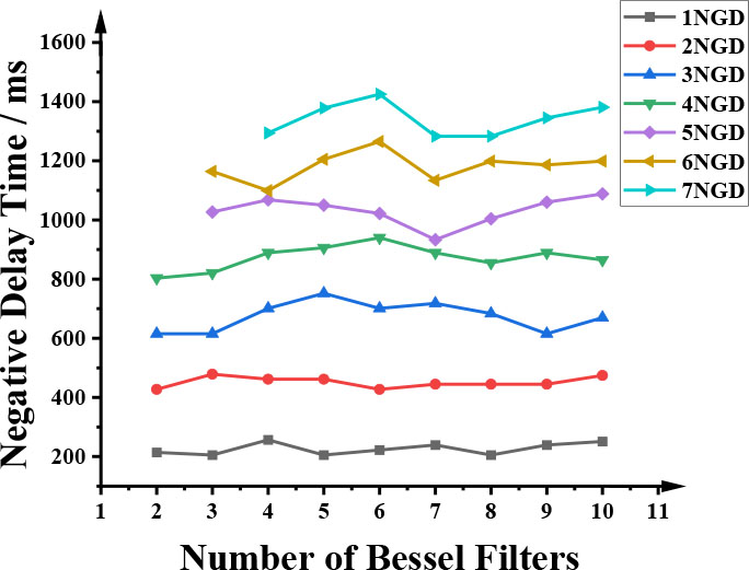
Figure 15.
The change of negative delay time with the number of Bessel filters under different number of negative group delay circuits
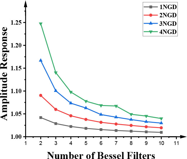
Figure 16.
The amplitude response varies with the number of Bessel filters under different number of negative group delay circuits
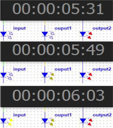
Figure 17.
LED simulation results