
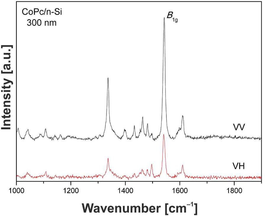
Fig. 1
Polarized Raman spectra (VV and VH) for CoPc thin layer deposited on Si substrate.
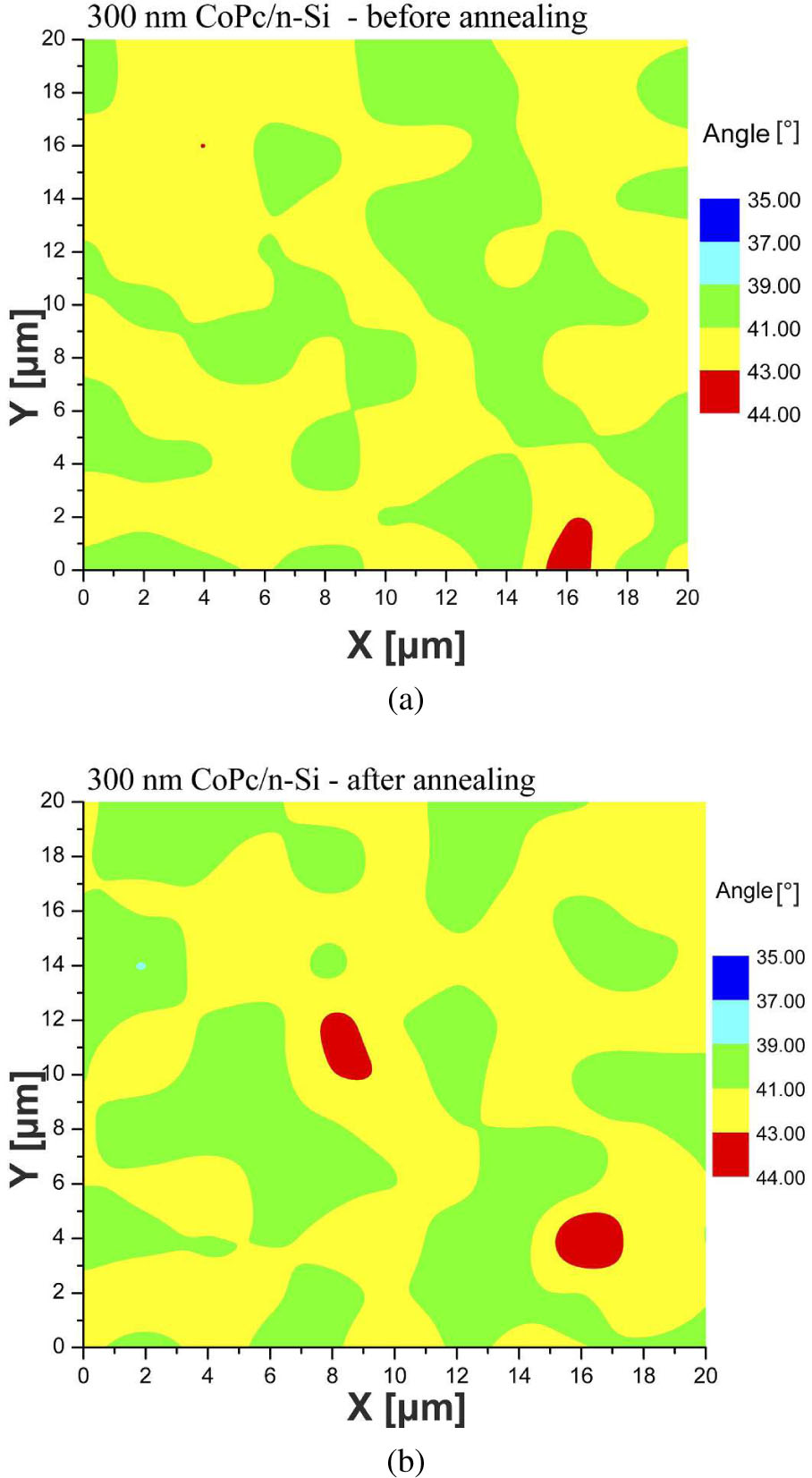
Fig. 2
Orientation of CoPc molecules (angle between molecule and substrate) obtained from Raman measurements (a) before and (b) after annealing process for 300 nm thick CoPc film.
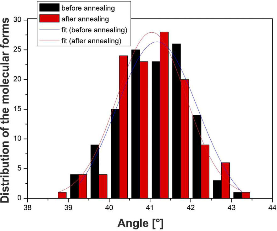
Fig. 3
Distribution of the molecular forms for CoPc thin layer obtained from Raman measurements before (black) and after (red) annealing.
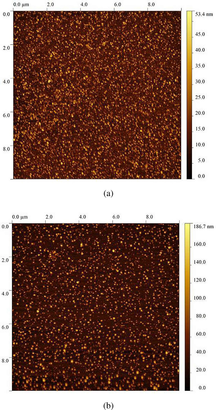
Fig. 4
AFM images for CoPc thin layer obtained for a) before and b) after annealing process.
Table 1
The surface parameters obtained from AFM images for CoPc thin film before and after annealing process.
| [nm] | Grain size | Ra | RMS | Avg. height | Max. height | Avg./Max. |
|---|---|---|---|---|---|---|
| before annealing | 71.37±14.65 | 4.99 | 6.37 | 13.01 | 53.40 | 0.244 |
| after annealing | 83.97±7.97 | 14.50 | 20.80 | 32.40 | 186.70 | 0.174 |
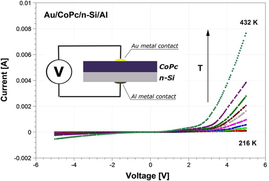
Fig. 5
Current-voltage characteristics (I-V) for CoPc thin layers before annealing; inset in Fig. 5 shows the electrical diagram.
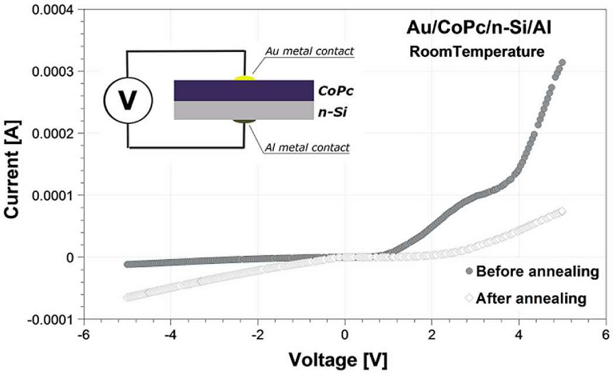
Fig. 6
Current-voltage characteristics (I-V) for CoPc thin layers before and after annealing process at the temperature of 473 K for 6 hours in air; the inset in Fig. 6 shows the electrical diagram.
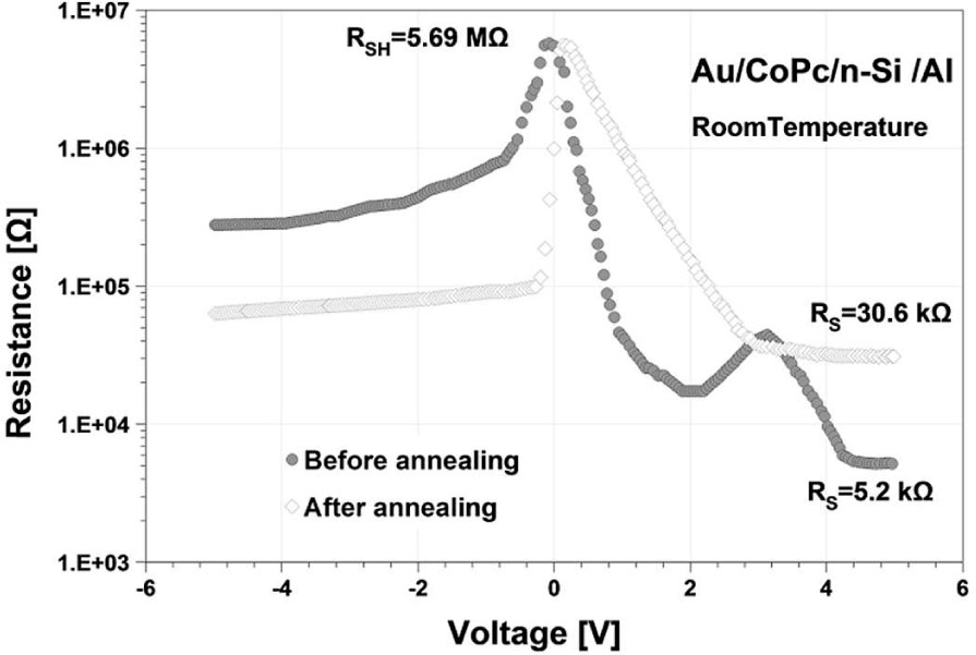
Fig. 7
Plots of junction resistance, Rj, against applied voltage at room temperature for Au/CoPc/n-Si/Al structure annealed at temperature of 473 K for 6 hours in air.