
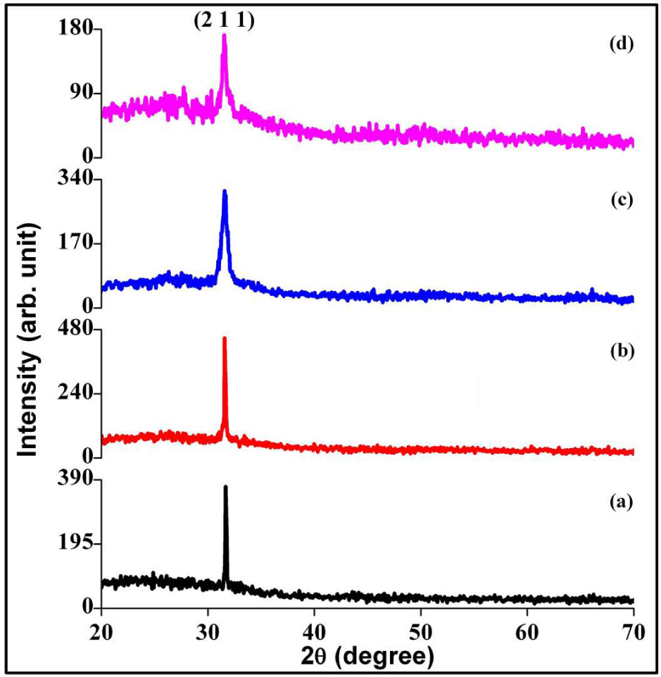
Fig. 1
XRD patterns of Sn2S3 thin films prepared with (a) 0.01:0.01, (b) 0.02:0.02, (c) 0.03:0.03 and (d) 0.04:0.04 S:Sn precursor molar concentrations.
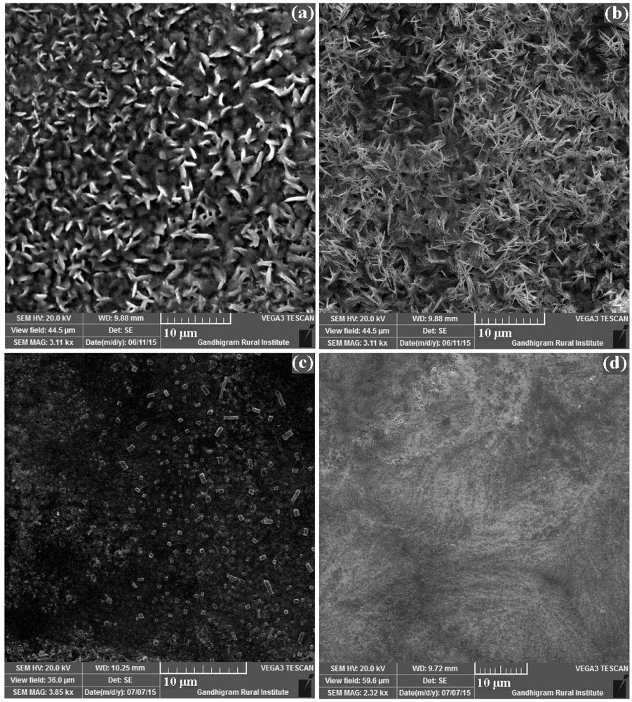
Fig. 2
SEM images of Sn2S3 thin films prepared with (a) 0.01:0.01, (b) 0.02:0.02, (c) 0.03:0.03 and (d) 0.04:0.04 S:Sn precursor molar concentrations.
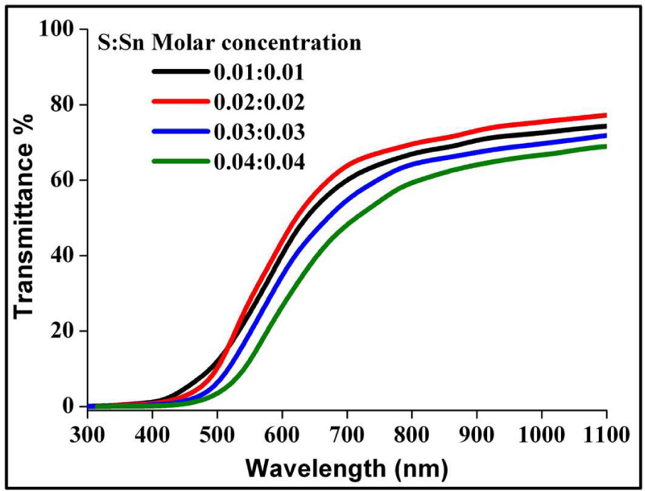
Fig. 3
Transmittance spectra of Sn2S3 thin films.
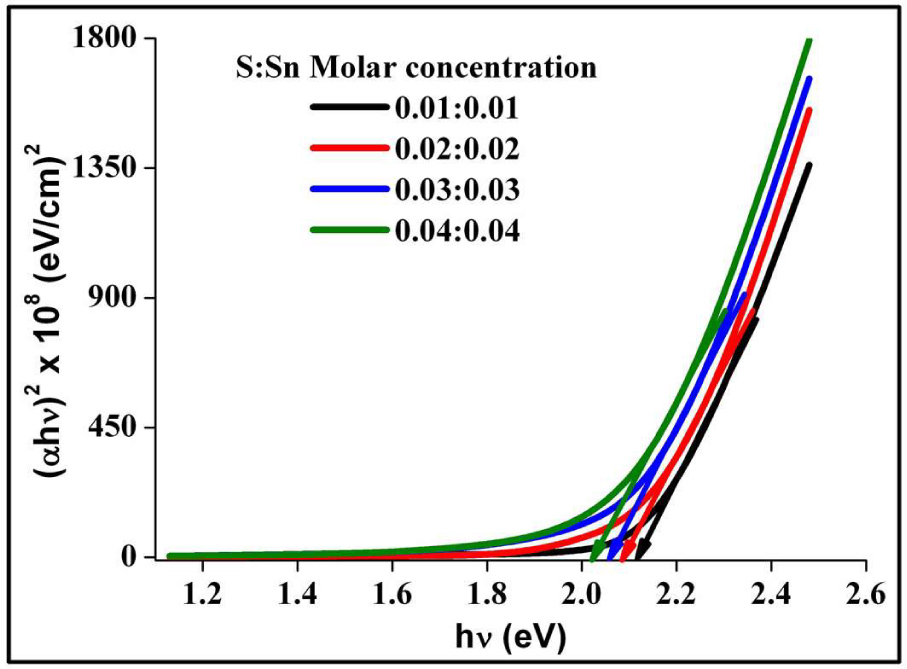
Fig. 4
Tauc’s plots of Sn2S3 thin films.
Table 1
Thickness, structural parameters and electrical resistivity values of Sn2S3 thin films prepared from solutions having different S:Sn precursor molar concentrations.
| S:Sn precursor | Thickness | d(211) | D | ε × 10−4 | δ × 10−14 | Lattice parameters [Å] | ρ | ||
|---|---|---|---|---|---|---|---|---|---|
| molar concentration | t [nm] | [Å] | [nm] | [lines/m2] | a | b | c | [Ω·cm] | |
| 0.01:0.01 | 90 | 2.8099 | 45.9 | 0.755 | 4.7489 | 15.554 | 5.620 | 5.659 | 0.238 |
| 0.02:0.02 | 122 | 2.8115 | 56 | 0.619 | 3.1931 | 15.563 | 5.623 | 5.662 | 0.359 |
| 0.03:0.03 | 176 | 2.8136 | 42 | 0.826 | 5.6773 | 15.575 | 5.627 | 5.666 | 1.095 |
| 0.04:0.04 | 206 | 2.8231 | 35.6 | 1.032 | 8.8709 | 15.627 | 5.646 | 5.685 | 6.38 |
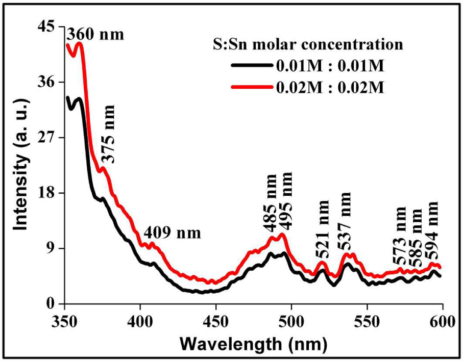
Fig. 5
PL spectra of Sn2S3 thin films coated with 0.01:0.01 and 0.02:0.02 S:Sn precursor molar concentrations.