

Figure 1.
SC balancing (a), DTSC balancing (b). DTSC, double-tiered switched-capacitor; SC, switched-capacitor.
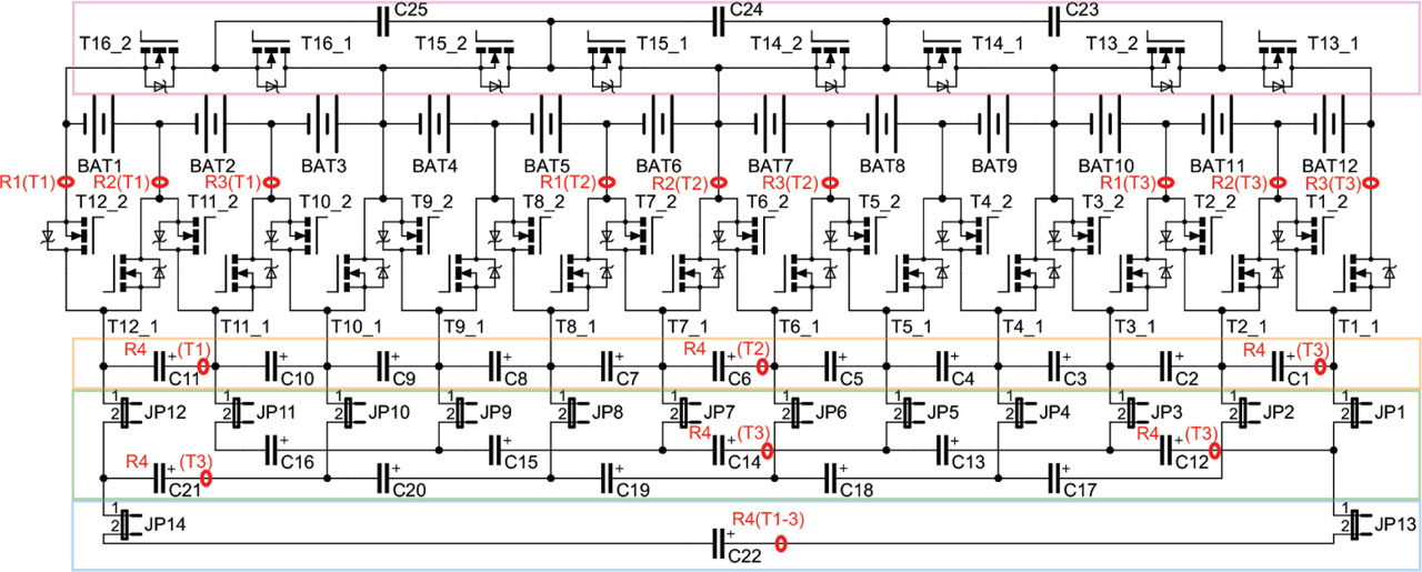
Figure 2.
Proposed balancing circuit diagram with different topologies: R1–R4 nodes with current measurement (0.1–0.3 for each test placement), orange – SC, green – DTSC, blue – DTSCAC, pink – MSC. DTSC, double-tiered switched-capacitor; DTSCAC, double-tiered switched-capacitor with an additional capacitor; MSC, modular switched-capacitor; SC, switched-capacitor.
Table 1.
Battery pack and balancing circuit parameters.
| Parameter group | Parameter | Value | Unit |
|---|---|---|---|
| Battery cell | Cell chemistry | LFP (APR18650M1B) | - |
| Nominal voltage | 3.3 | V | |
| Rated capacity | 1.2 | Ah | |
| Internal resistance (range) | 16.8–18.3 | mΩ | |
| Charging voltage | 3.6 | V | |
| Charging current | 1.5 | A | |
| Charge termination @ 3.6 V | <50 | mA | |
| Battery pack (12S1P) | Number of cells | 12 (in series) | - |
| Nominal voltage | 40 | V | |
| Charging voltage (12 in parallel) | 3.6 | V | |
| Charging current | 6, 15 | A | |
| Charge termination @ 3.6 V | <0.5–0.7 | A | |
| Charging method | CCCV | - | |
| Balancing circuit | Topology | SC/DTSC/DTSCAC | - |
| Capacitor capacitance | 10,000/10,000/2 × 2,200 | µF | |
| Switching frequency | 1 | kHz |

Figure 3.
Balancer block diagram (left) and full experimental balancer setup with wiring (right) – 1. Oscilloscope Tektronix MSO4034, 2. Power supply 24 V for the cooling fan, 3. Power supply 3.6 V for charging battery cells, 4. Current probe amplifier Tektronix TCPA300, 5. Battery module, 6. Voltage measuring board Infineon TLE9012DQU, 7. Control module with discharge unit, 8. Charger for battery cells (parallel), 9. Display for control module, 10. Cooling fan for discharge process, 11. Balancer module, 12,13. External DC/DC power supply for transistor gates, 14. Current probe Tektronix TCP312.
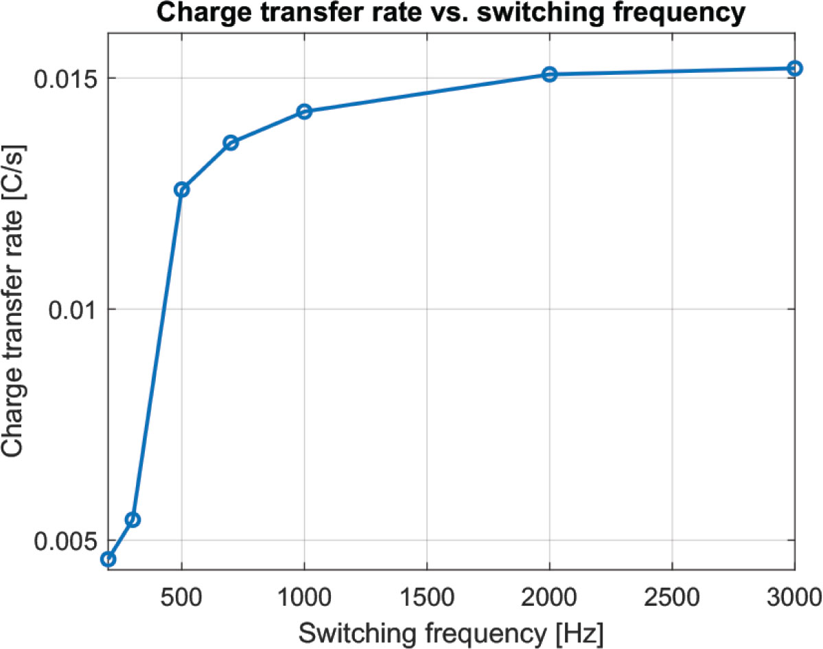
Figure 4.
Charge transfer rate as a function of switching frequency.
Table 2.
Charge transfer rate as a function of switching frequency.
| Switching frequency (Hz) | Charge transfer rate (C/s) |
|---|---|
| 200 | 0.004588 |
| 300 | 0.005441 |
| 500 | 0.012585 |
| 700 | 0.013600 |
| 1,000 | 0.014274 |
| 2,000 | 0.015079 |
| 3,000 | 0.015210 |
Table 3.
Definition of test scenarios with corresponding measurement points, topology, and balancing time needed to reach a 50 mV difference between the highest and the lowest cell.
| Topology | Test | Code | Highest cell | Lowest cell | R1 (node) | R2 (node) | R3 (node) | R4 (capacitor) | Average balancing time to 50 mV difference [s] |
|---|---|---|---|---|---|---|---|---|---|
| SC | T1.1 | 1H2L | Cell 1 | Cell 2 | Node 2 | Node 3 | Node 4 | C11 | 4,697 |
| SC | T2.1 | 1H6L | Cell 1 | Cell 6 | Node 6 | Node 7 | Node 8 | C6 | 8,969 |
| SC | T3.1 | 1H12L | Cell 1 | Cell 12 | Node 11 | Node 12 | Node 13 | C1 | 8,730 |
| DTSC | T1.2 | 1H2L | Cell 1 | Cell 2 | Node 2 | Node 3 | Node 4 | C21 | 5,216 |
| DTSC | T2.2 | 1H6L | Cell 1 | Cell 6 | Node 6 | Node 7 | Node 8 | C14 | 6,845 |
| DTSC | T3.2 | 1H12L | Cell 1 | Cell 12 | Node 11 | Node 12 | Node 13 | C12 | 8,540 |
| DTSCAC | T1.3 | 1H2L | Cell 1 | Cell 2 | Node 2 | Node 3 | Node 4 | C22 | 5,659 |
| DTSCAC | T2.3 | 1H6L | Cell 1 | Cell 6 | Node 6 | Node 7 | Node 8 | C22 | 9,300 |
| DTSCAC | T3.3 | 1H12L | Cell 1 | Cell 12 | Node 11 | Node 12 | Node 13 | C22 | 8,868 |
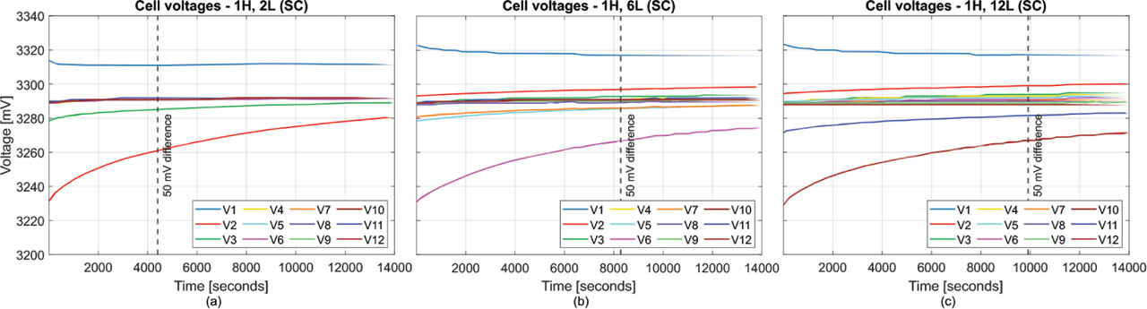
Figure 5.
Voltage equalisation of 12S1P battery pack during balancing with SC topology: (a) Test T1.1, (b) Test T2.1, (c) Test T3.1. SC, switched-capacitor.
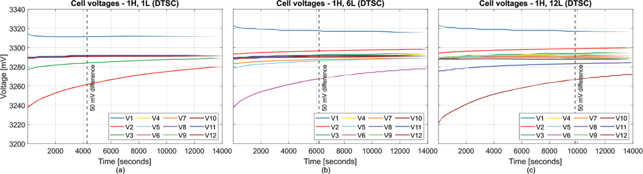
Figure 6.
Voltage equalisation of 12S1P battery pack during balancing with DTSC topology: (a) Test T1.2, (b) Test T2.2, (c) Test T3.2. DTSC, double-tiered switched-capacitor.
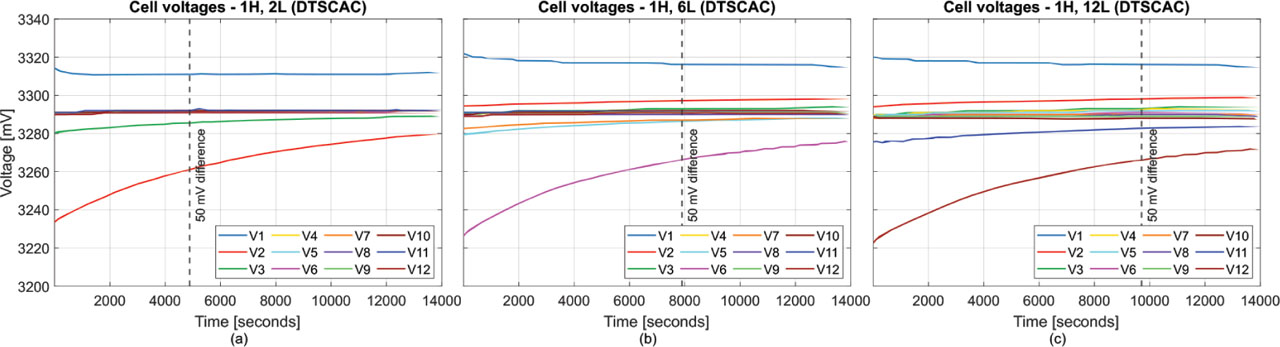
Figure 7.
Voltage equalisation of 12S1P battery pack during balancing with DTSCAC topology: (a) Test T1.3, (b) Test T2.3, (c) Test T3.3. DTSCAC, double-tiered switched-capacitor with an additional capacitor.
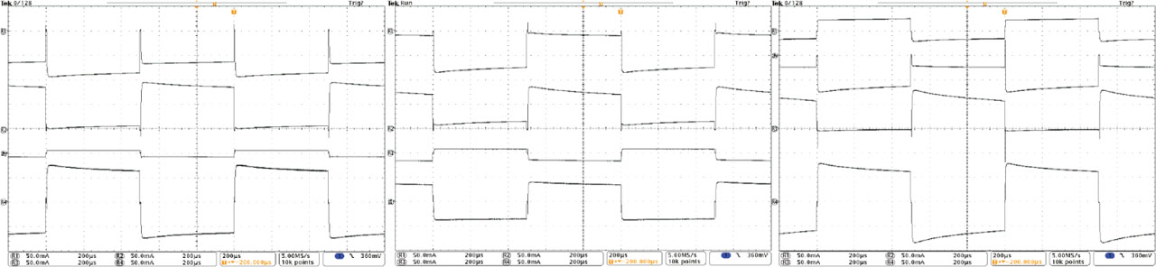
Figure 8.
Node current waveforms for SC topology: (left) Test T1, (middle) Test T2, (right) Test T3 – nodes described in Table 3. SC, switched-capacitor.
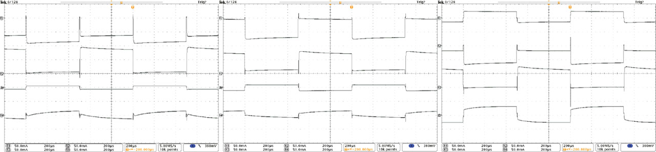
Figure 9.
Node current waveforms for DTSC topology: (left) Test T1, (middle) Test T2, (right) Test T3 – nodes described in Table 3. DTSC, double-tiered switched-capacitor.
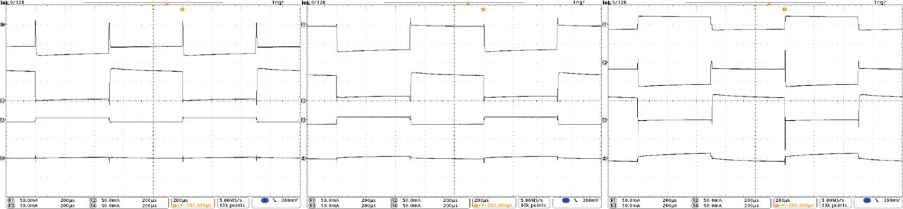
Figure 10.
Node current waveforms for DTSCAC topology: (left) Test T1, (middle) Test T2, (right) Test T3 – nodes described in Table 3. DTSCAC, double-tiered switched-capacitor with an additional capacitor.