
Figure 1.

Figure 2.

Figure 3.
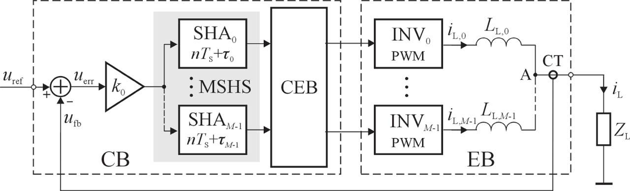
Figure 4.

Figure 5.

Figure 6.
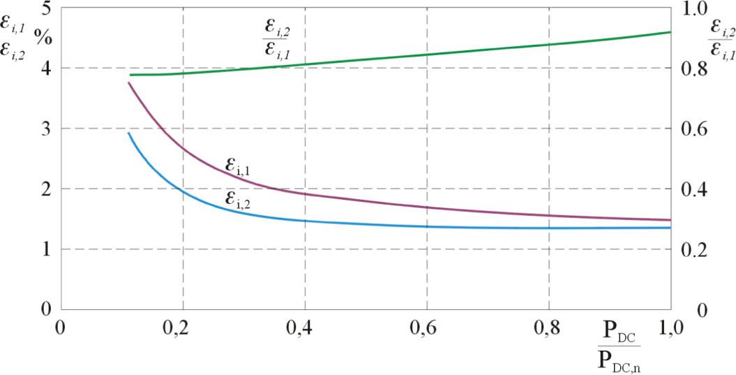
Figure 7.
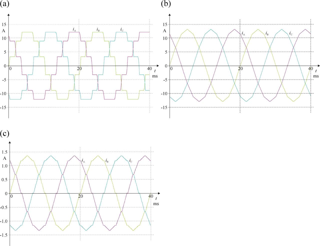
Figure 8.
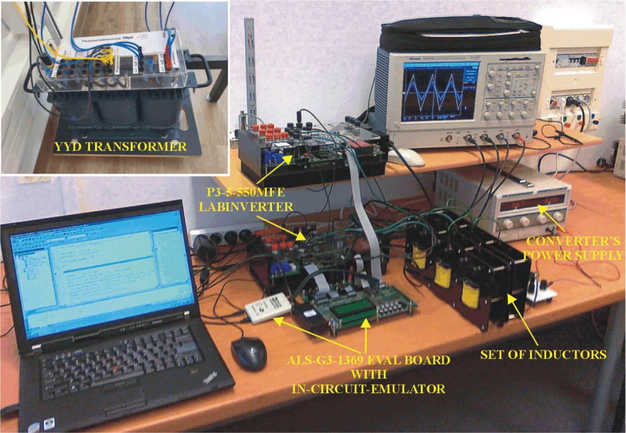
Figure 9.
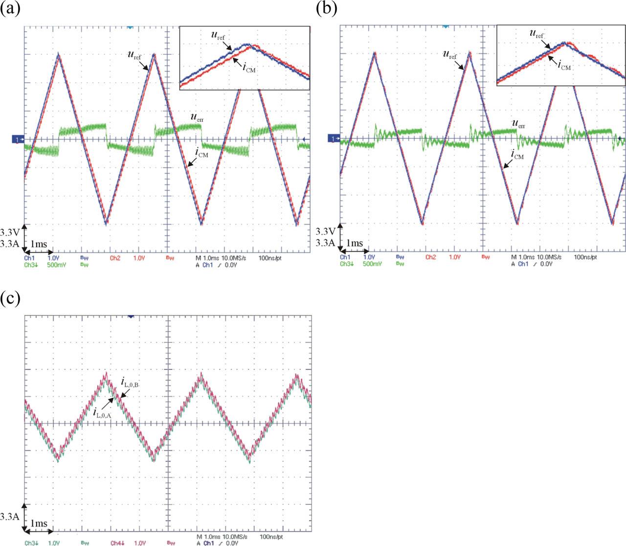
Figure 10.

Parameters of the laboratory setup_
| Parameters | Values |
|---|---|
| Power supply | 230V, 50 Hz |
| Rated power delivered to the load | 6 kW |
| Rated current magnitude at the modulator output | 10 A |
| Voltage in the current modulation stage (DC rails) | 60V |
| Coil inductance in an individual channel of the VCCS | 1.25 mH |
| Frequency of the PWM signal in the VCCS execution unit | 10 kHz |
| Frequency of signal sampling in the VCCS controller unit | 10 kHz |