
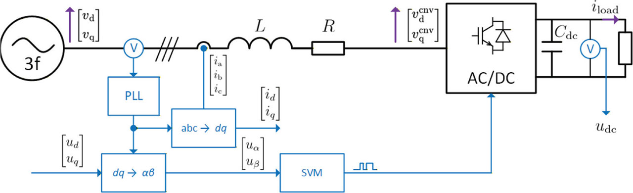
Figure 1.
Block diagram of the plant. PLL, phase-locked loop.
Table 1.
Parameters of grid GCC.
| Parameter name | Symbol | Value |
|---|---|---|
| Nominal grid voltage (RMS) | Vn | 400 V |
| Nominal grid current (RMS) | In | 14 A |
| Nominal grid frequency | fn | 50 Hz |
| Input filter inductance | L | 2 mH |
| Input filter resistance | R | 0.1 Ω |
| DC-link capacitance | Cdc | 500 μF |
| Switching/sampling frequency | fsw | 10 kHz |
| Nominal DC voltage | 600 V | |
| Nominal load current | 16.2 A |
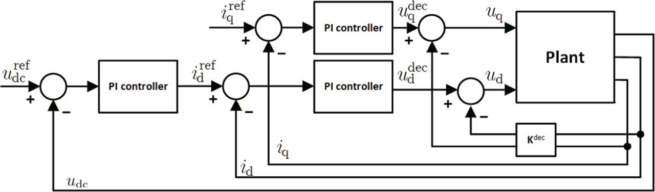
Figure 2.
Block diagram of a cascade control structure with PI controllers.
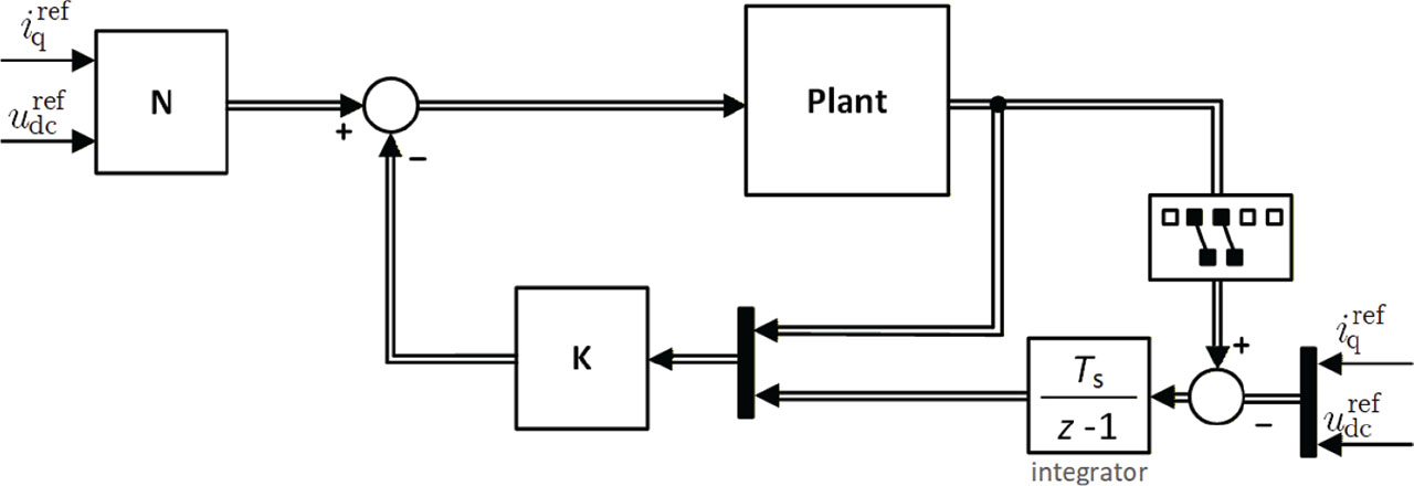
Figure 3.
Block diagram of the full state feedback control structure.
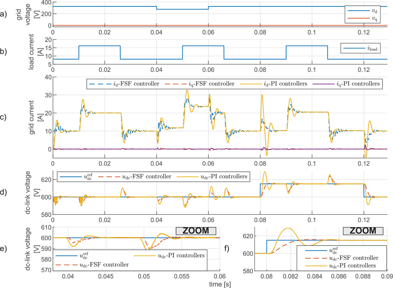
Figure 4.
Numerical simulation comparison of the considered control systems represented in synchronous frame: a) grid voltage, b) load current, c) grid current, d) dc-link voltage e) and f) zoom on dc-link voltage.
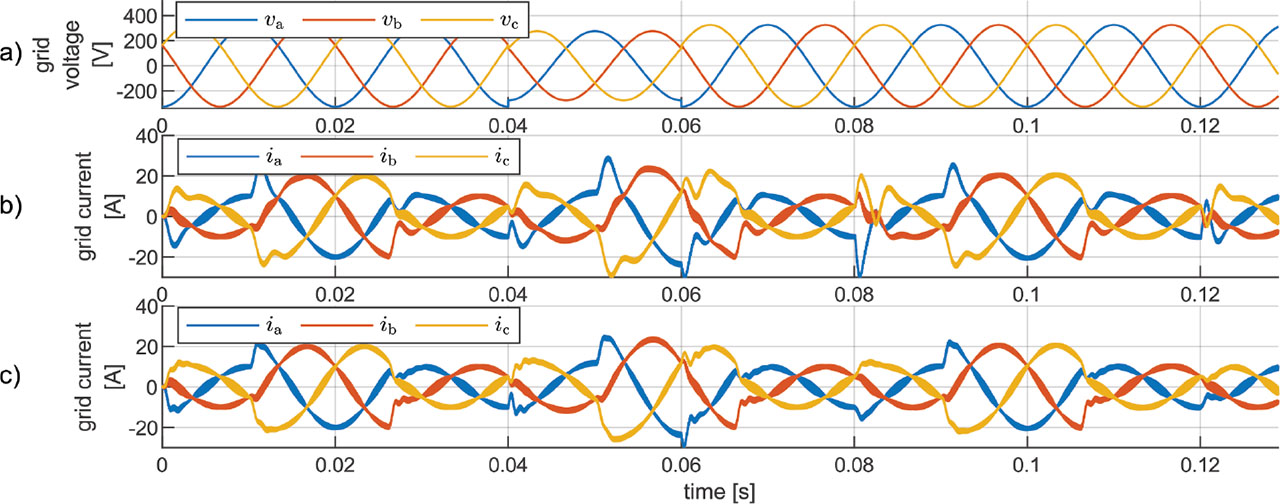
Figure 5.
Simulation results illustrating in the stationary frame the performance differences between the two control strategies: a) grid voltage, b) grid current – PI-controller-based cascade structure, c) grid current – FSF control structure.
Table 2.
Comparison of the control properties of PI-controller-based and FSF control structures
| Performance metric | Cascade PI control | FSF control |
|---|---|---|
| Settling time | Fast | Fast |
| Voltage sag – disturbance rejection | Effective | Highly effective |
| Step load – disturbance rejection | Effective, moderate oscillations | Effective, well-dumped response |
| Reference step response | High DC voltage overshoot, High peak current, oscillatory response | Low DC voltage overshoot, moderate peak current, well-dumped response |
Figure 6.
Simulation results illustrating in the stationary frame the performance differences between the two control strategies: a) grid voltage, b) grid current – PI controller based cascade structure, c) grid current – FSF control structure.
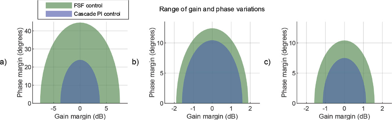
Figure 7.
Disk-based stability margins of the control system for a) input perturbation, b) output perturbation, c) simultaneous input and output perturbation.
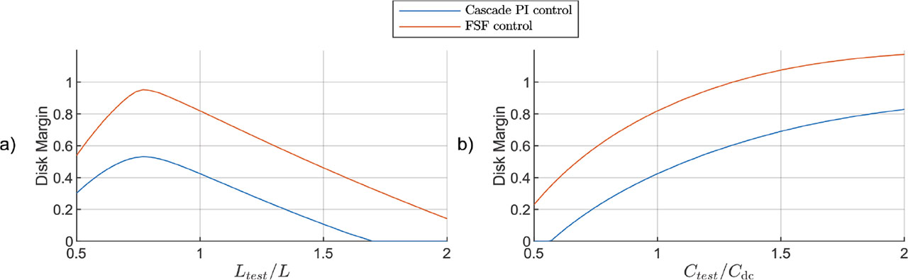
Figure 8.
Effect of input filter inductance (a) and DC-link capacitance (b) variations on the stability margin.
Table 3.
DM based stability analysis results
| Performance metric | DMs at plant inputs | DMs at plant outputs | DM at both inputs and outputs | |
|---|---|---|---|---|
| Cascade PI control | Disk size | 0.4245 | 0.1827 | 0.1311 |
| Gain margin | [0.6499 1.5388] | [0.8326 1.2010] | [0.8770 1.1402] | |
| Phase margin | [−23.9640 23.9640] | [−10.4367 10.4367] | [−7.4982 7.4982] | |
| FSF control | Disk size | 0.8196 | 0.2175 | 0.1822 |
| Gain margin | [0.4186 2.3887] | [0.8038 1.2440] | [0.8330 1.2004] | |
| Phase margin | [−44.5681 44.5681] | [−12.4128 12.4128] | [−10.4088 10.4088] |