
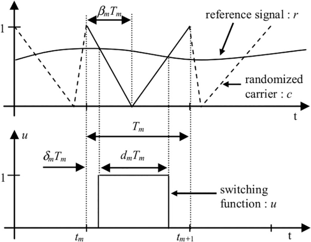
Figure 1.
Modulating principle of RPWM. RPWM, random pulse width modulation.
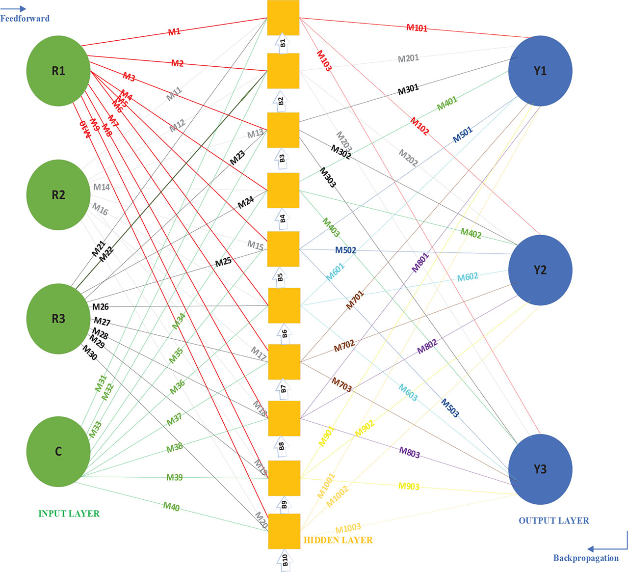
Figure 2.
ANN architecture. ANN, artificial neural network.
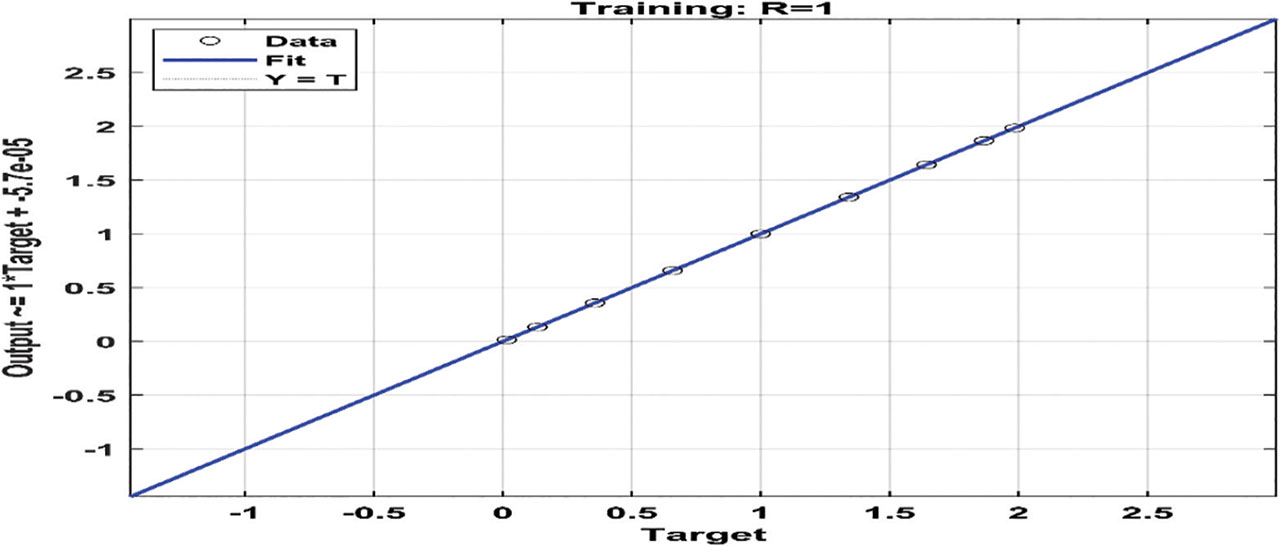
Figure 3.
Output regression line after training.
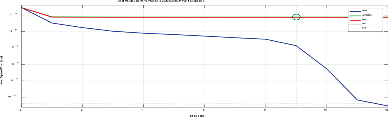
Figure 4.
MSE output curve after training. MSE, mean squared error.
Table 1.
ANN training parameters.
| Parameters | Values |
|---|---|
| Network type | Feedforward/backpropagation |
| Learning algorithm | Trainlm |
| Epochs | 1,000 |
| Convergence limit (Goal) | 1e−12 |
| Hidden layers | 10 |
| Input layers | 4 |
| Output layers | 3 |
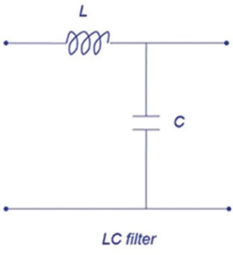
Figure 5.
Single line diagram of LC low pass filter.
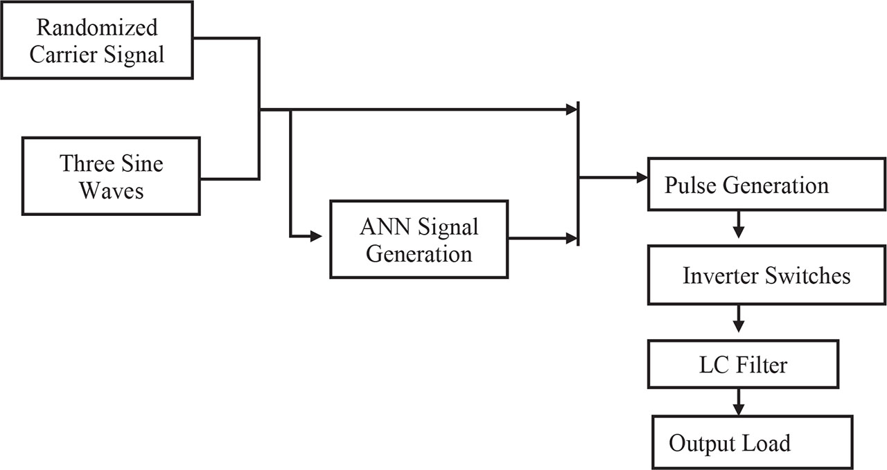
Figure 6.
Block diagram of the proposed method. ANN, artificial neural network.
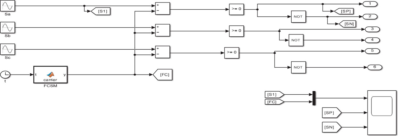
Figure 7.
Switching pulse generation for FCSM. FCSM, fixed carrier signal modulated.
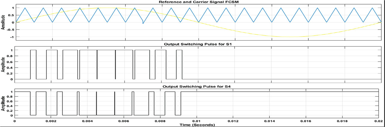
Figure 8.
Pulse generation for the FCSM strategy on one leg of three phase inverter. FCSM, fixed carrier signal modulated.
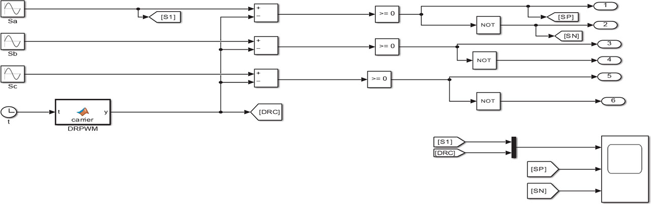
Figure 9.
Switching pulse generation for DRPWM. DRPWM, dual random pulse width modulated.
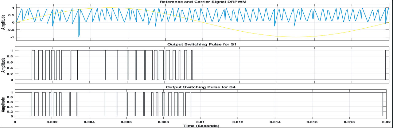
Figure 10.
Pulse generation for the DRPWM strategy on one leg of three phase inverter. DRPWM, dual random pulse width modulated.
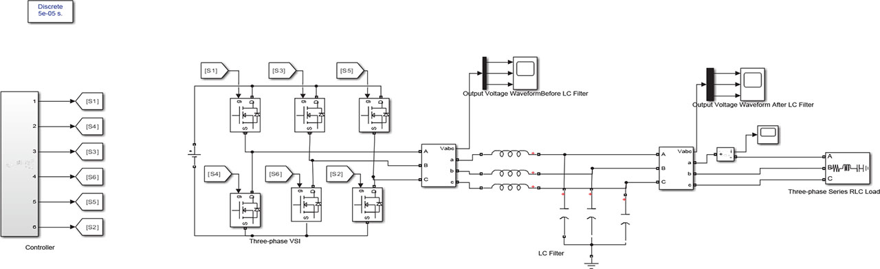
Figure 11.
Diagram of the three-phase VSI. VSI, voltage source inverter.
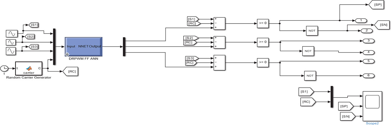
Figure 12.
Pulse generation for ANN incorporated. ANN, artificial neural network.
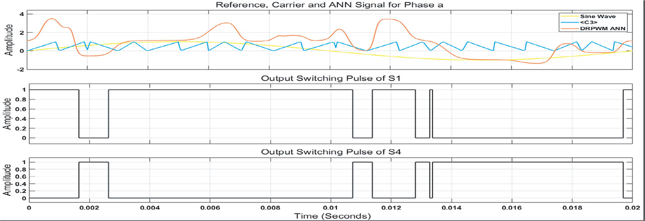
Figure 13.
Pulse generation for the proposed strategy on one leg of three-phase inverter. ANN, artificial neural network; DRPWM, dual random pulse width modulated.
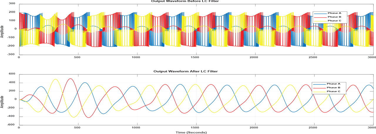
Figure 14.
Output voltage waveform with and without an LC filter for FCSM. FCSM, fixed carrier signal modulated.
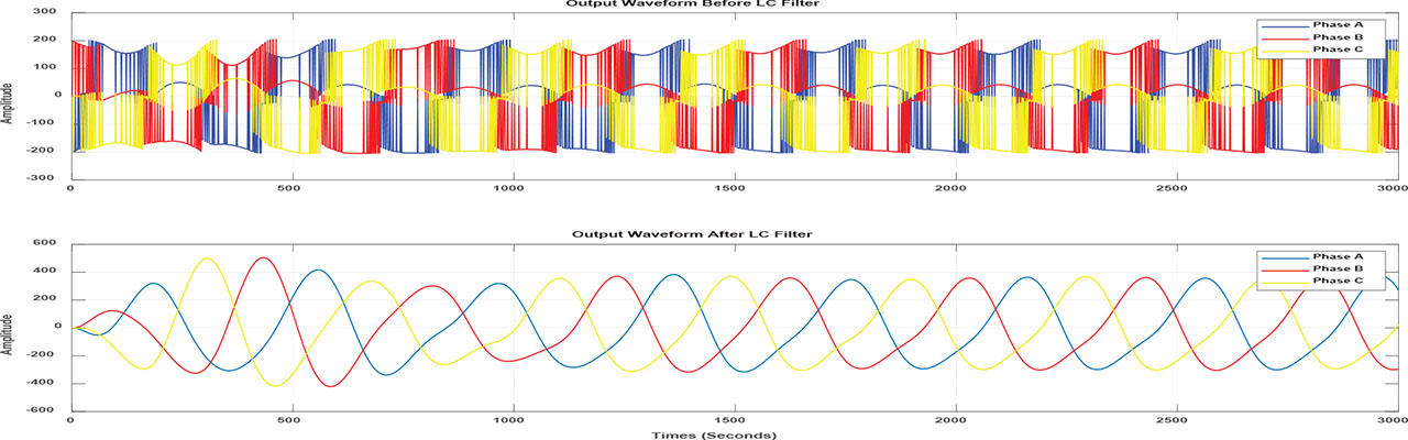
Figure 15.
Output voltage waveform with and without LC filter for DRPWM. DRPWM, dual random pulse width modulated.
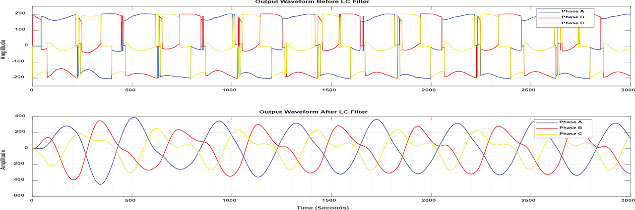
Figure 16.
Output voltage waveforms before and after the LC filter for the proposed method.
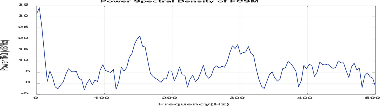
Figure 17.
Output voltage PSD of FCSM. FCSM, fixed carrier signal modulated; PSD, power spectral density.
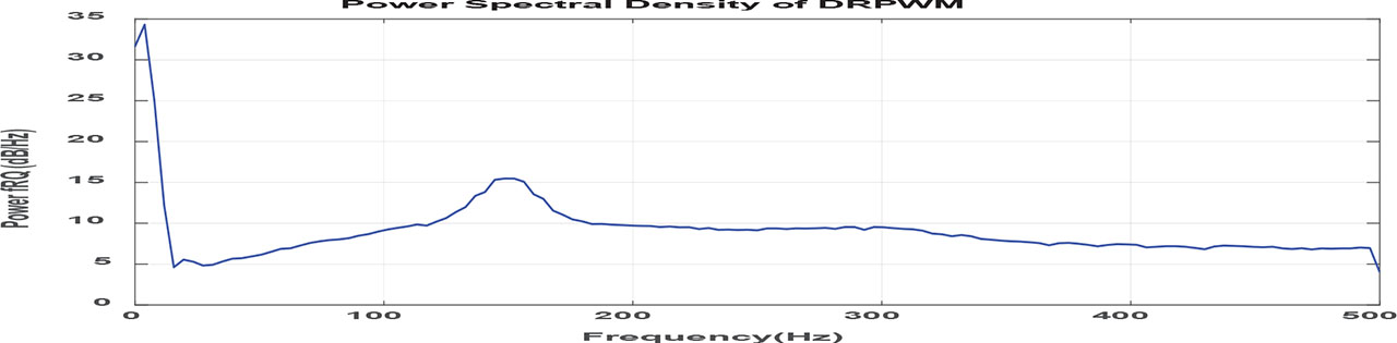
Figure 18.
Output voltage PSD of DRPWM. DRPWM, dual random pulse width modulated; PSD, power spectral density.
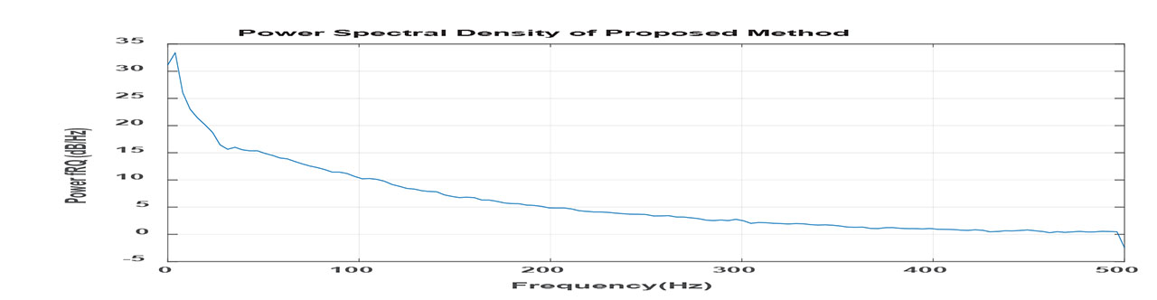
Figure 19.
Output voltage PSD of the proposed method. PSD, power spectral density.
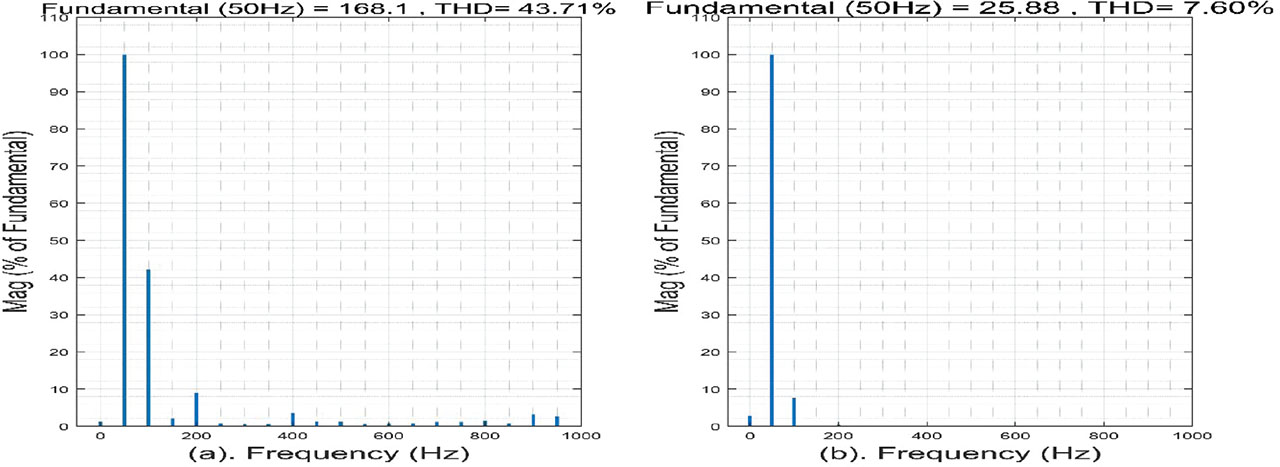
Figure 20.
THD content of the FCSM. (a) Before and (b) after the LC filter. FCSM, fixed carrier signal modulated; THD, total harmonic distortion.
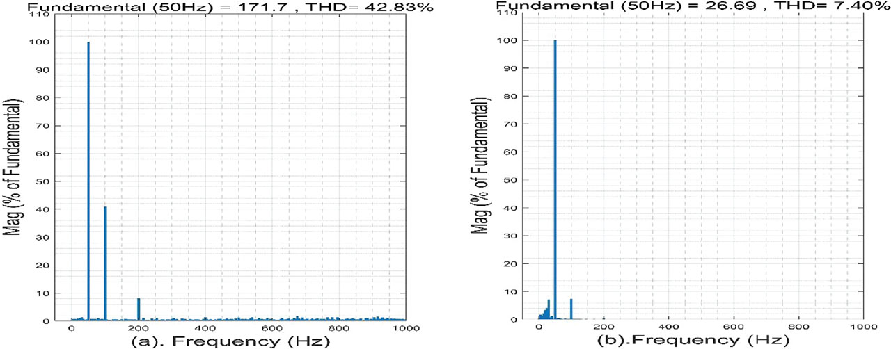
Figure 21.
THD content of the DRPWM (a). Before and (b). After the LC filter. DRPWM, dual random pulse width modulated; THD, total harmonic distortion.
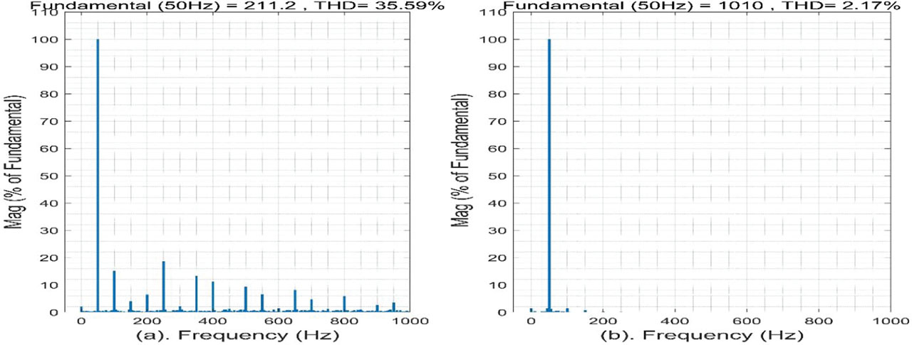
Figure 22.
THD content of the proposed method. (a) Before and (b) After the LC filter. THD, total harmonic distortion.
Table 2.
Summary of THD content levels (%).
| System | THD before filter (%) | THD after LC filter (%) |
|---|---|---|
| FCSM | 43.71 | 7.60 |
| DRPWM | 42.83 | 7.40 |
| Proposed method | 35.59 | 2.17 |
Table 3.
Summary of harmonics and their relative magnitudes.
| Harmonic order | FCSM (dB) | DRPWM (dB) | ANN-RPWM (dB) | Reduction vs. DRPWM (%) |
|---|---|---|---|---|
| 5 | −36 | −40 | −46 | 43 |
| 7 | −38 | −42 | −47 | 37 |
| 11 | −40 | −43 | −48 | 35 |
| 13 | −42 | −44 | −49 | 35 |
Table 4.
Techno-economic comparison between conventional RPWM and proposed ANN-RPWM controller.
| Cost component | Conventional RPWM system | Proposed ANN–RPWM system | Remarks/assumptions |
|---|---|---|---|
| DSP/microcontroller | Included | Same | No additional processor required |
| Power semiconductors (IGBTs/drivers) | 6 IGBTs + 3 drivers | Same | Unchanged hardware configuration |
| Sensors/feedback circuits | 3 V, 3 current sensors | Same | No modification needed |
| Software/algorithmic overhead | Baseline PWM control | +3% additional CPU load | ANN inference executed on the same DSP |
| Development/training effort | N/A | One-time offline training | Conducted using MATLAB on PC |
| Filter components (L, C) | LC filter | Same | Identical filter design used |
| Implementation/maintenance | Standard | Standard | No extra calibration required |
| Estimated total cost impact | 100% | ≈101% | <1% incremental difference |