
Fig. 1.
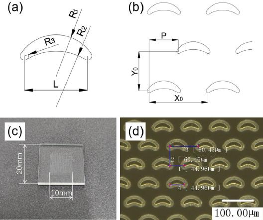
Fig. 2.
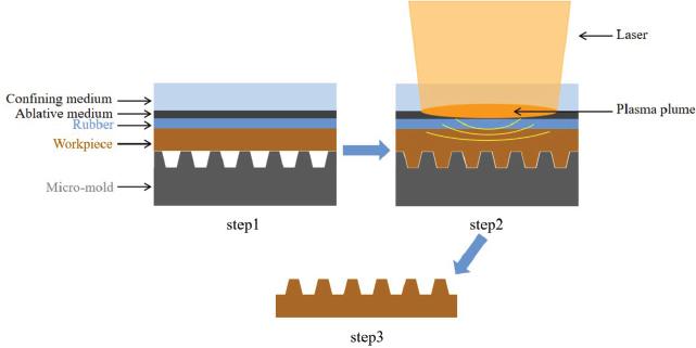
Fig. 3.
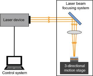
Fig. 4.
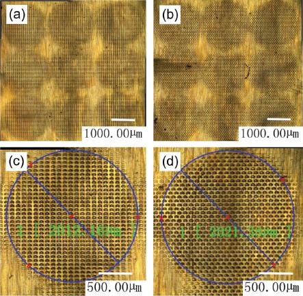
Fig. 5.
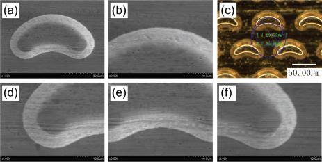
Fig. 6.
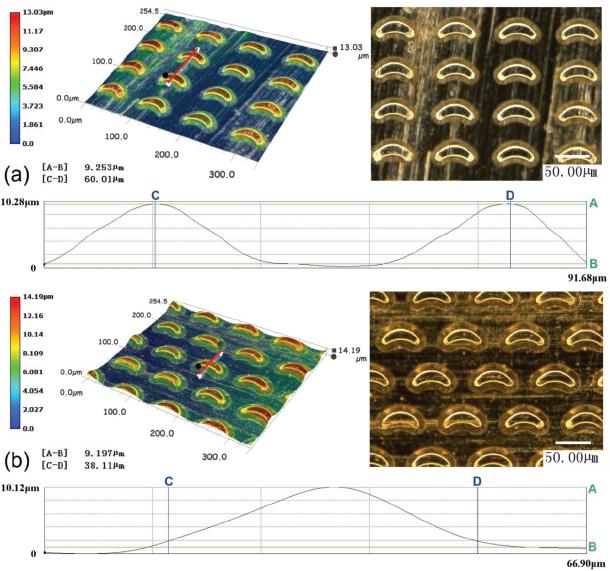
Fig. 7.
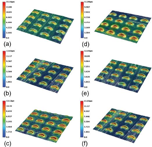
Fig. 8.
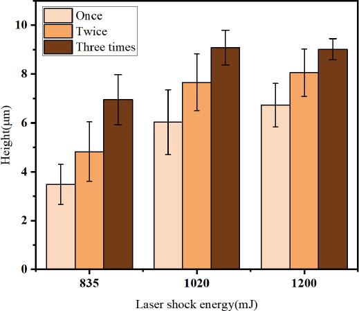
Fig. 9.
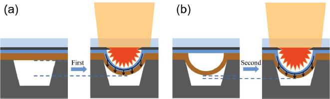
Fig. 10.
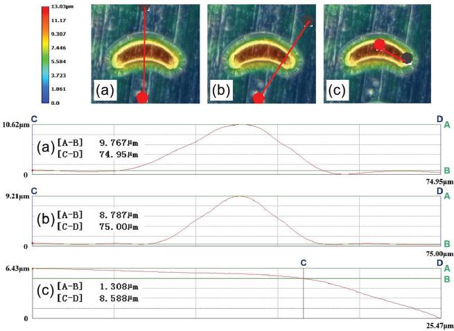
Fig. 11.
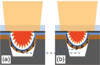
Fig. 12.
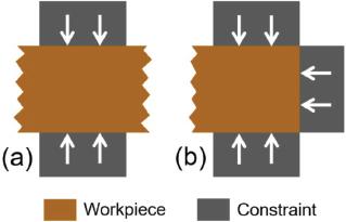
Fig. 13.
Fig. 14.
Fig. 15.
Fig. 16.
Fig. 17.
Fig. 18.
Fig. 19.
Fig. 20.
Fig. 21.
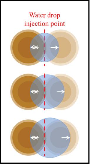
Fig. 22.
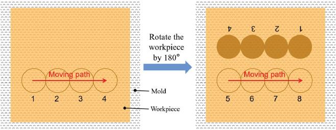
Fig. 23.
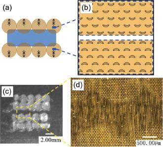
Fig. 24.
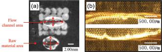
Fig. 25.
Process parameters for LSI
| LSE1 (mJ) | Number of laser shocks (times) | ||
|---|---|---|---|
| 835 | 1 | 2 | 3 |
| 1020 | 1 | 2 | 3 |
| 1200 | 1 | 2 | 3 |
Materials for LSI
| Functionality | Constraint layer | Ablative layer | Soft film | Workpiece |
|---|---|---|---|---|
| Material | PMMA | Aluminum foil | Polyurethane | Copper foil |
| Thickness | 3 mm | 20 μm | 100 μm | 10 μm |
Parameters of the fabricated molds
| Mold | P | L | R1 | R2 | R3 | X0 | Y0 |
|---|---|---|---|---|---|---|---|
| type | (μ m) | (μ m) | (μ m) | (μ m) | (μ m) | (μ m) | (μ m) |
| Mold 1 | 0 | 45 | 30 | 36 | 4 | 90 | 60 |
| Mold 2 | 30 | ||||||
| Mold 3 | 45 |