
Fig. 1
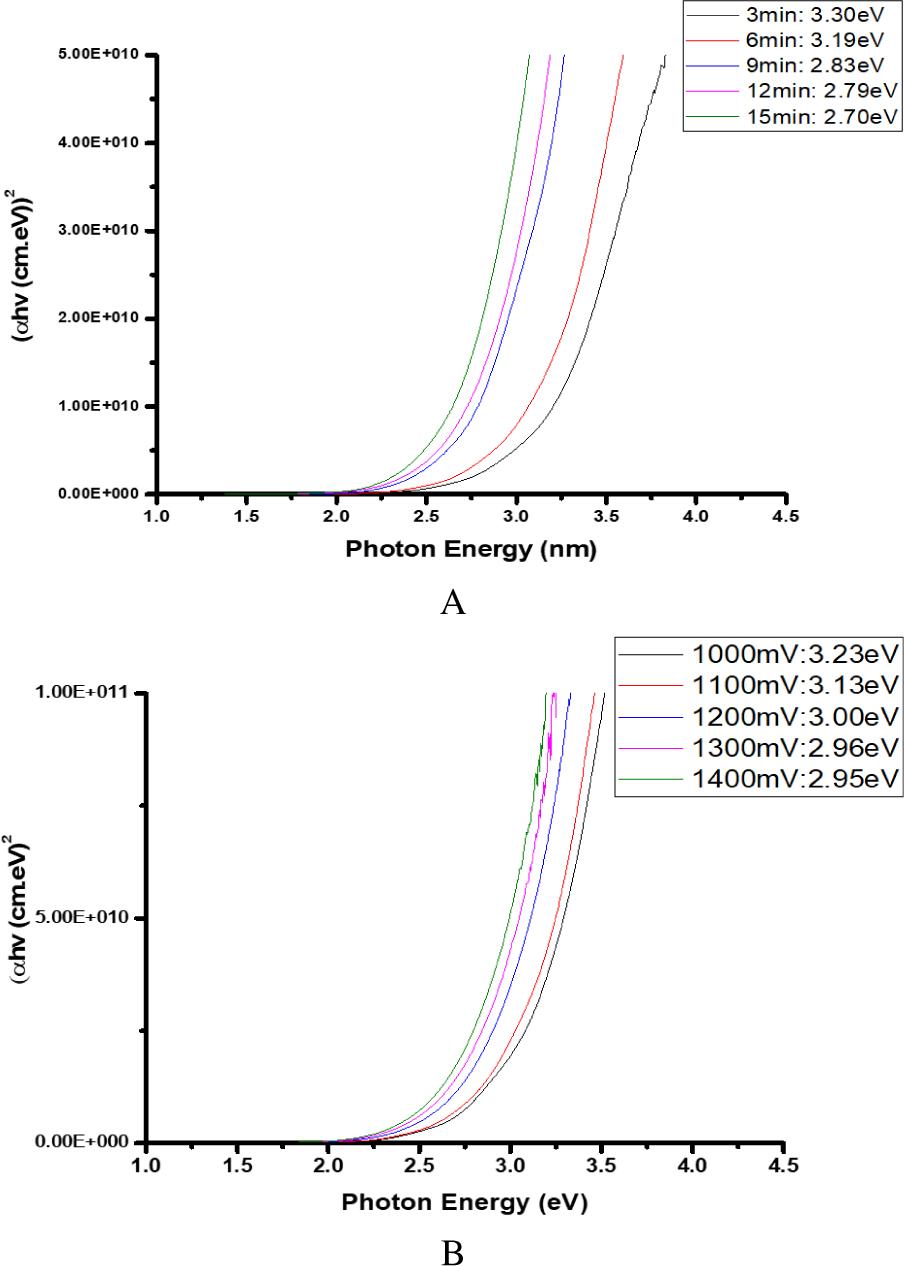
Fig. 2
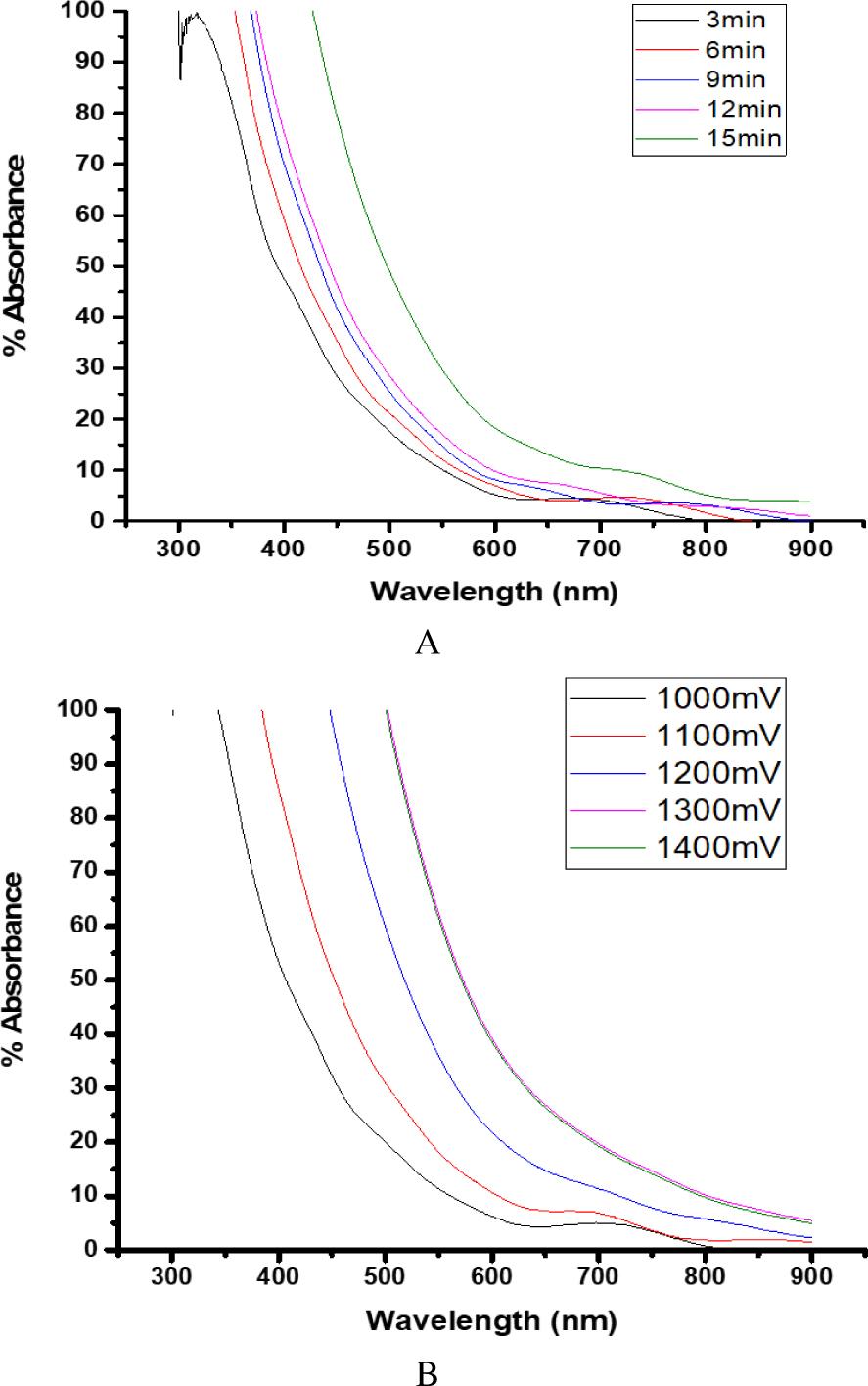
Fig. 3
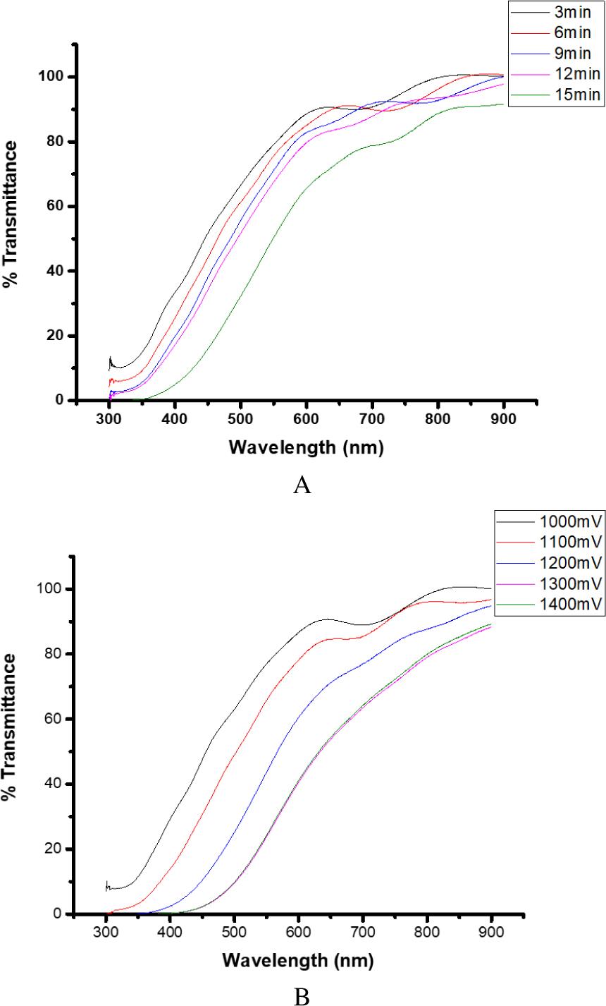
Fig. 4
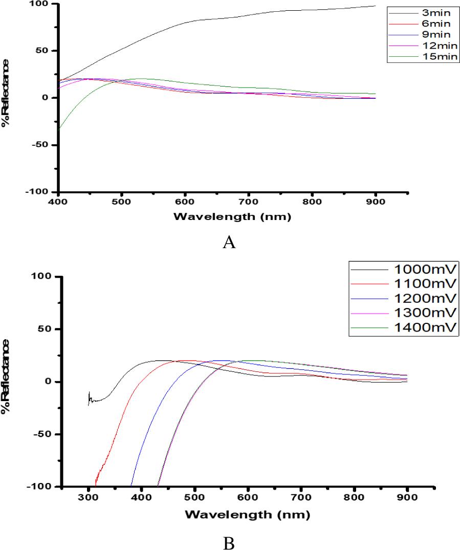
Fig. 5
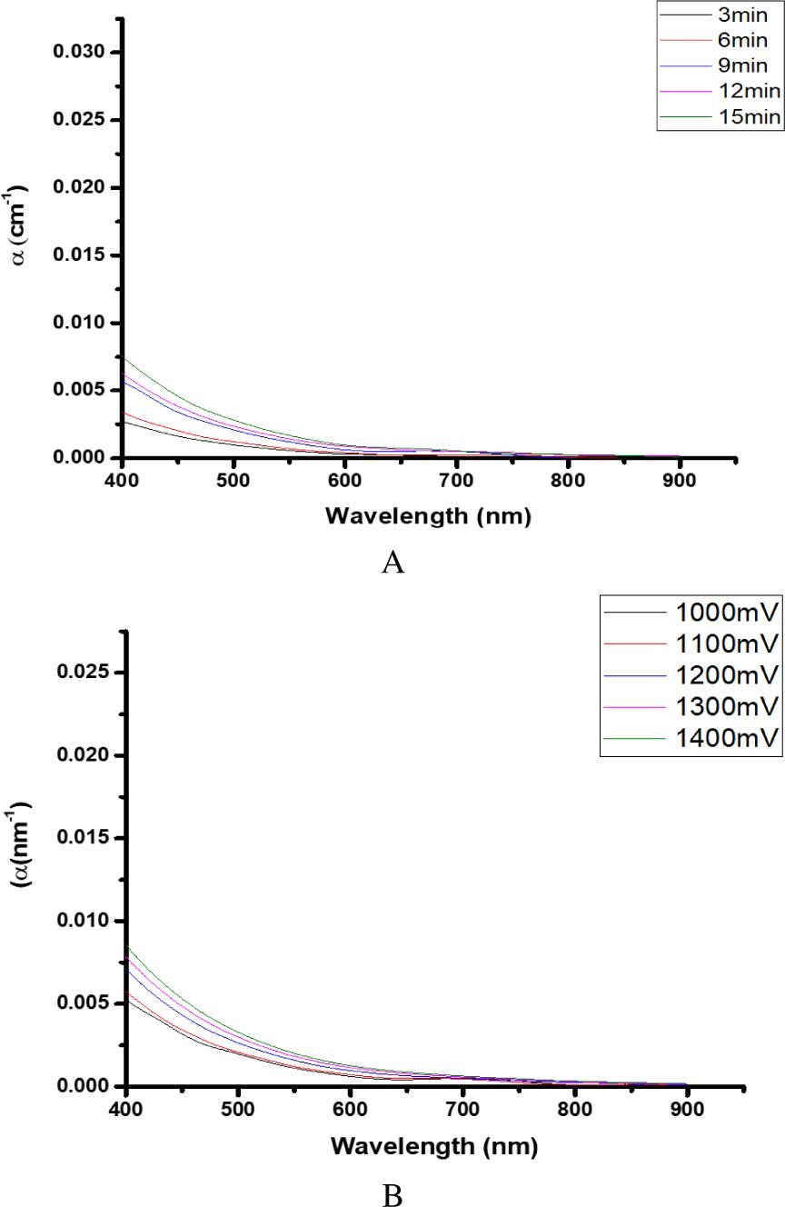
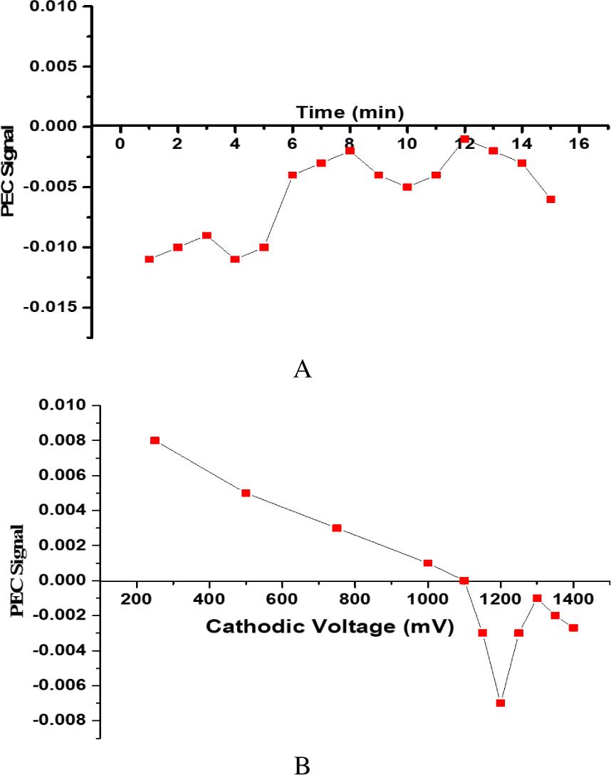
Fig. 6
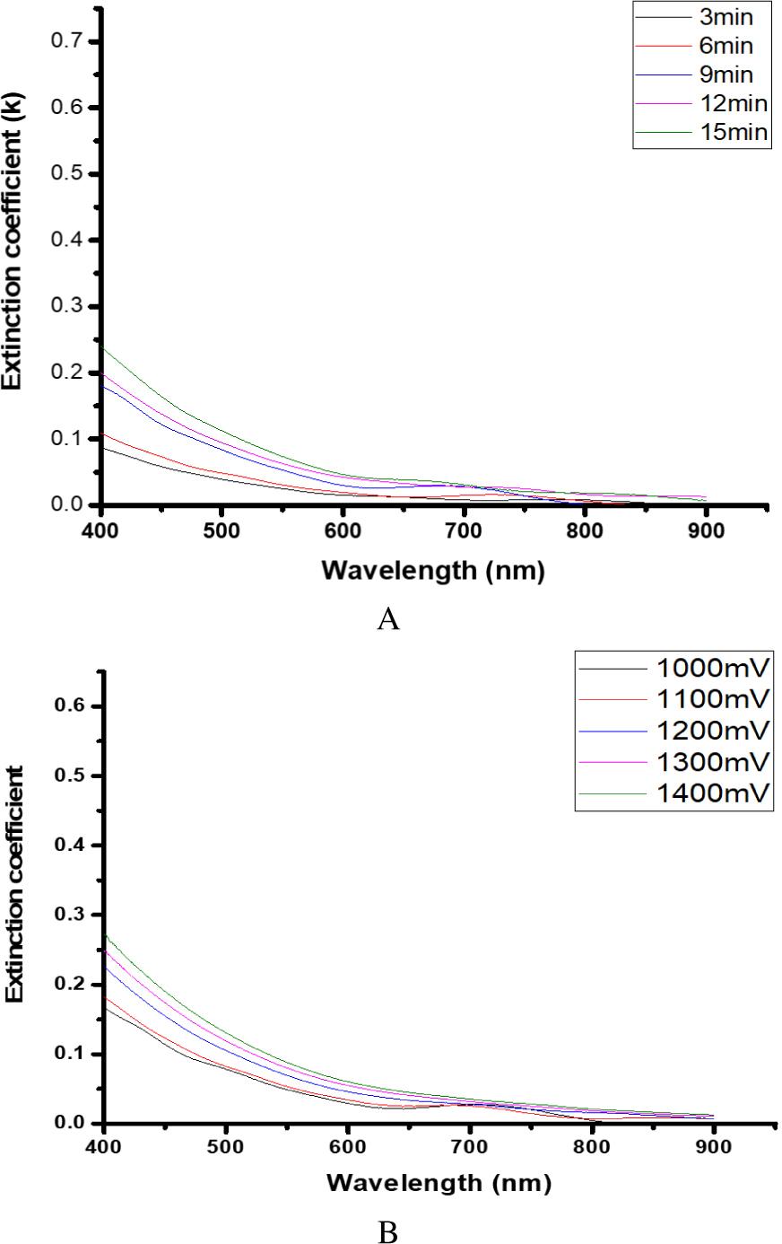
Fig. 7
Film thickness values with the variation in the time of deposition and cathodic potential_
| Film thickness as the time of deposition increases | Film thickness as the cathodic potential increases | ||
|---|---|---|---|
| Time (min) | Thickness (nm) | Cathodic potential (mV) | Thickness (nm) |
| 3 | 193 | 1,000 | 234 |
| 6 | 233 | 1,100 | 344 |
| 9 | 399 | 1,200 | 522 |
| 12 | 476 | 1,300 | 714 |
| 15 | 592 | 1,400 | 773 |
Measured material properties as a function of deposition time and cathodic potential based on UV and PEC results_
| Semiconductor type and energy band gaps | |||||
|---|---|---|---|---|---|
| As time of deposition increases | As voltage increases | ||||
| Time (min) | Type | Eg (eV) | Cathodic potential (mV) | Type | Eg (eV) |
| 3 | N | 3.30 | 1,000 | P | 3.23 |
| 6 | N | 3.19 | 1,100 | I-Intrinsic | 3.20 |
| 9 | N | 2.83 | 1,200 | N | 3.00 |
| 12 | N | 2.79 | 1,300 | N | 2.96 |
| 15 | N | 2.70 | 1,400 | N | 2.95 |