
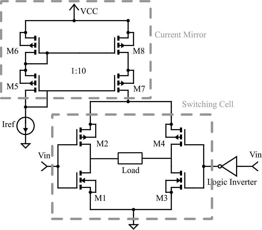
Figure 1:
SCMOSCS Schematic Diagram.
Table 1:
Transistor dimensions used in simulation
| MOSFET | L (μm) | W (μm) |
|---|---|---|
| M1 and M3 | 1 | 40 |
| M2 and M4 | 1 | 120 |
| M5 and M6 | 2 | 48 |
| M7 and M8 | 2 | 480 |
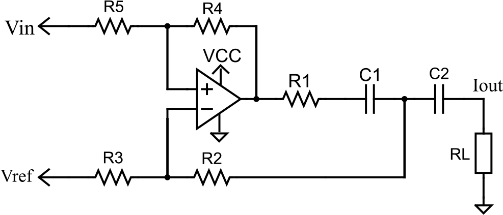
Figure 2:
Enhanced Howland Current source Schematic.
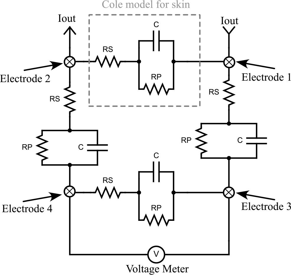
Figure 3:
Load arrangement using cole model.
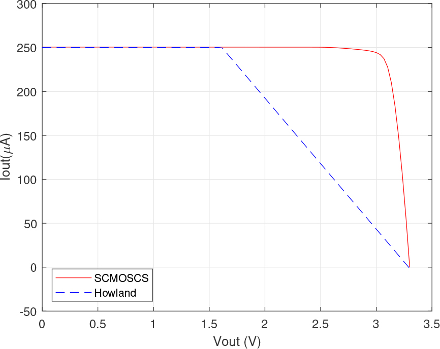
Figure 4:
DC analysis results of the Output current versus output voltage.
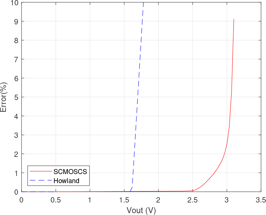
Figure 5:
DC analysis results of the output current relative error versus output voltage.
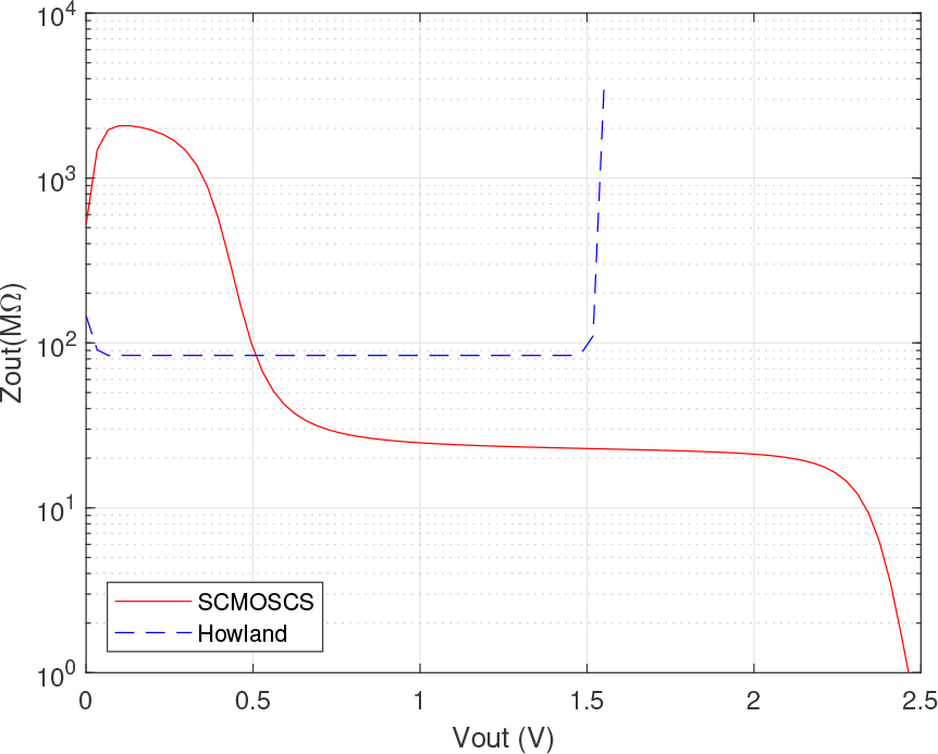
Figure 6:
DC analysis results of the output impedance versus output voltage.
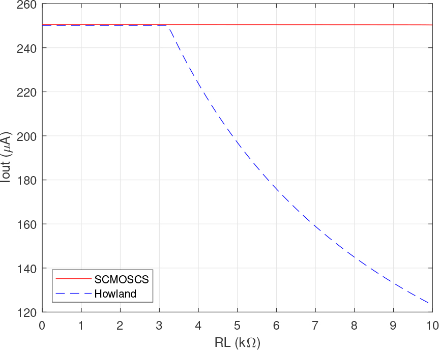
Figure 7:
DC analysis results of the output current versus load resistance
Table 2:
CC output current (in μA) considering temperature and voltage supply corners
| Topology | lout (0 < T < 100°C) | lout (1.8 < VCC < 3.3 V) |
|---|---|---|
| EHCS | 250.118 to 250.121 | 249.97 to 250.12 |
| SCMOSCS | 250.35 to 250.22 | 247.95 to 250.33 |
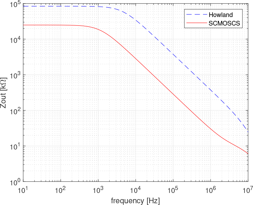
Figure 8:
Output impedance versus frequency in AC analysis.
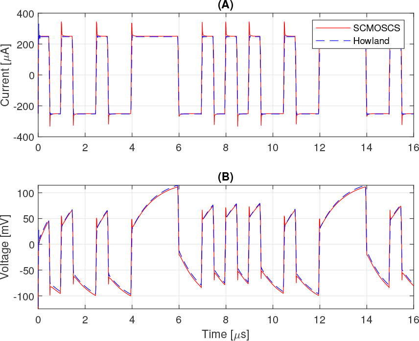
Figure 9:
Transient analysis of: (A) output current and (B) output voltage.
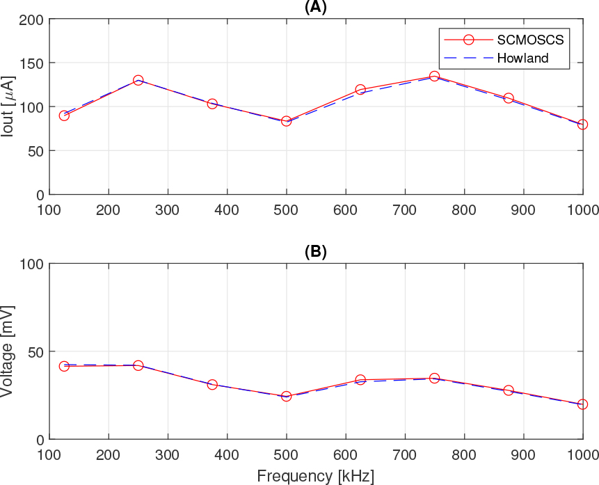
Figure 10:
Spectra as function of frequency of: (A) output current and (B) output voltage.
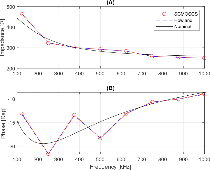
Figure 11:
Impedance spectra as a function of frequency.