
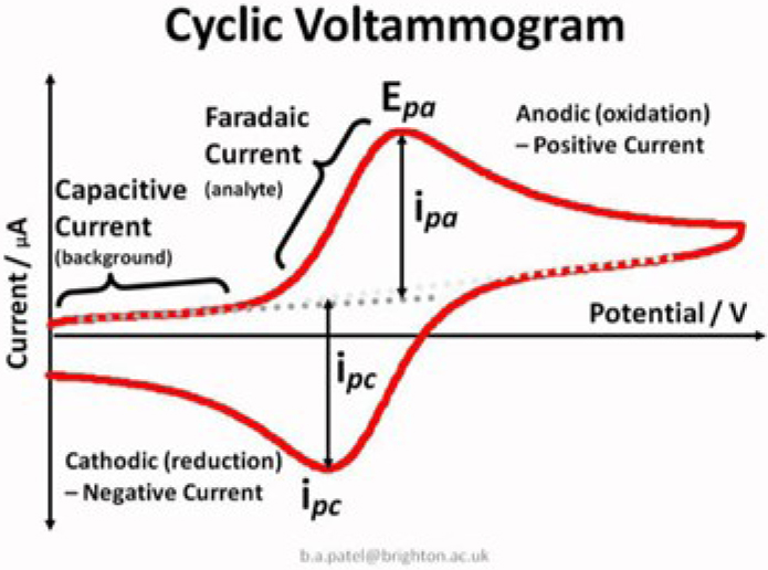
Fig. 1
CV graph with forward and reverse scan [From 5]
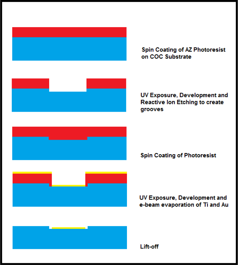
Fig. 2
Process flow of gold electrode fabrication
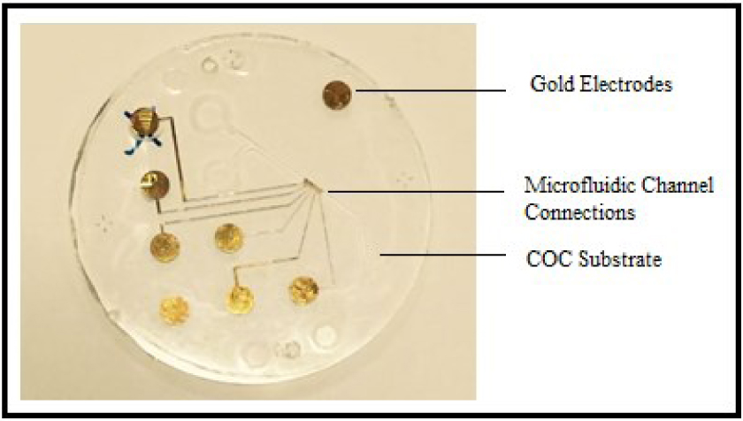
Fig. 3
Gold electrode fabricated on COC substrate
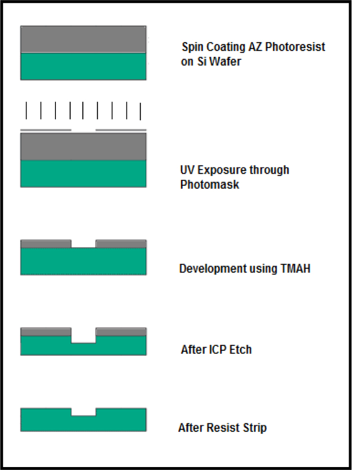
Fig. 4
Process flow of photolithography process for silicon mold
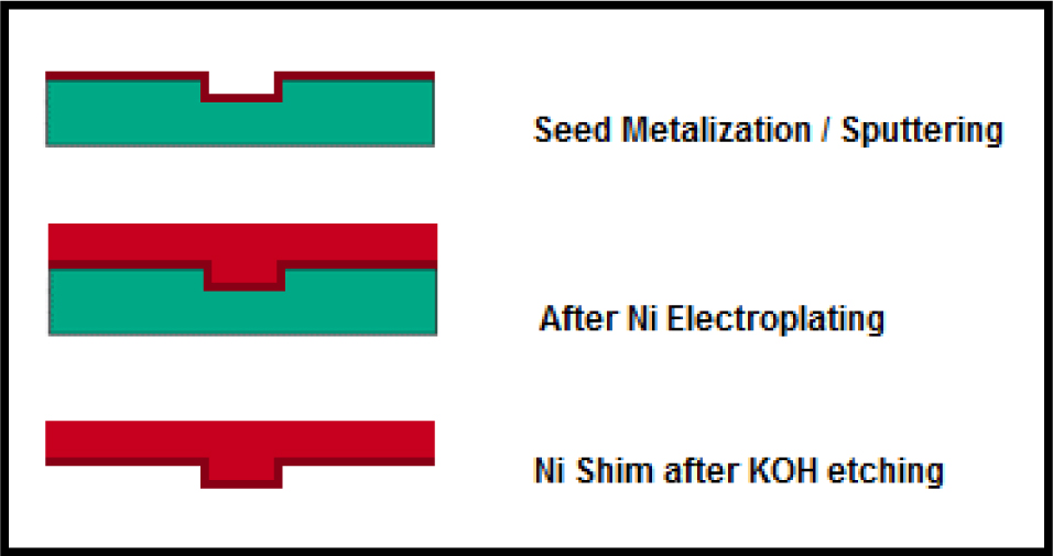
Fig. 5
Process flow of Nickle shim fabrication
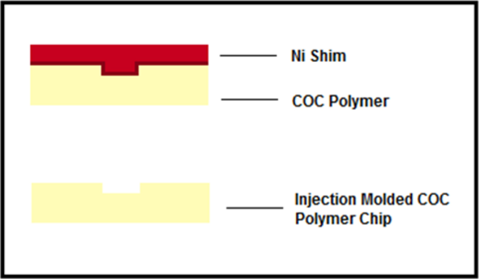
Fig. 6
Process flow of injection molded chip
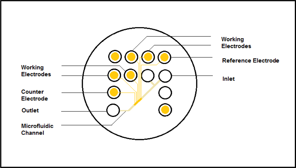
Fig. 7
Schematic of complete fabricated chip
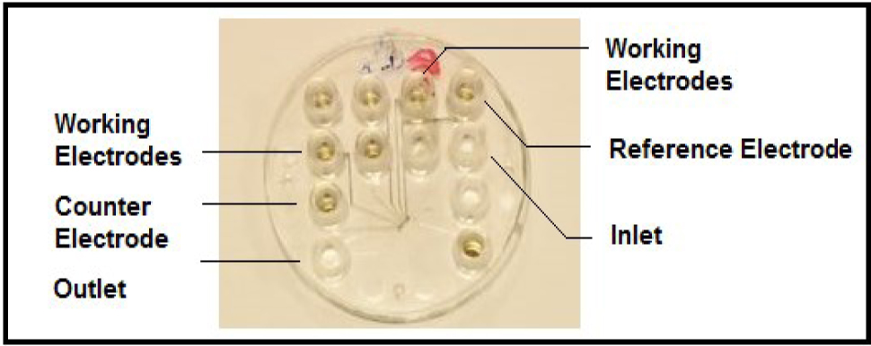
Fig. 8
Complete chip after fabrication and bonding
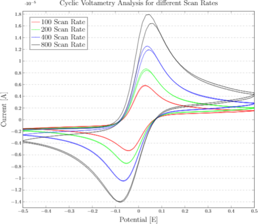
Fig. 9
Cyclic voltammograms at different scan rates for uncleaned thermally bonded chip
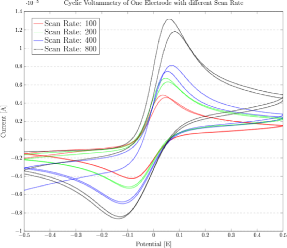
Fig. 10
Cyclic voltammograms at different scan rates for cleaned (with KOH) thermally bonded chip
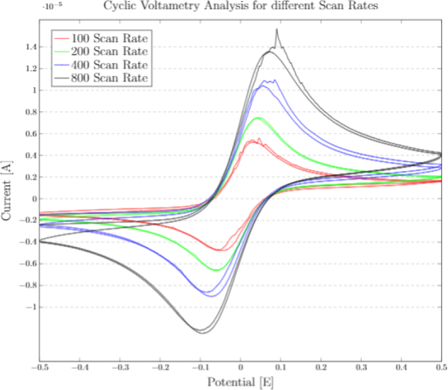
Fig. 11
Cyclic voltammograms at different scan rates for uncleaned ultrasonically welded chip
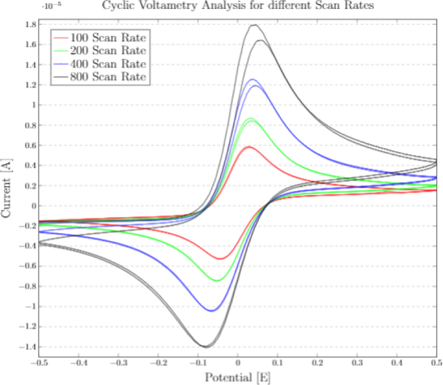
Fig. 12
Cyclic Voltammograms at different scan rates for cleaned (with KOH) ultrasonically welded chip
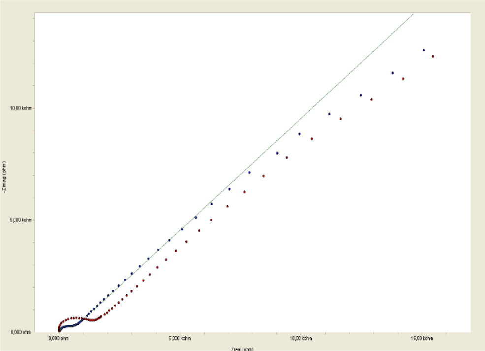
Fig. 13
Impedance spectroscopy for cleaned and uncleaned thermally bonded chip
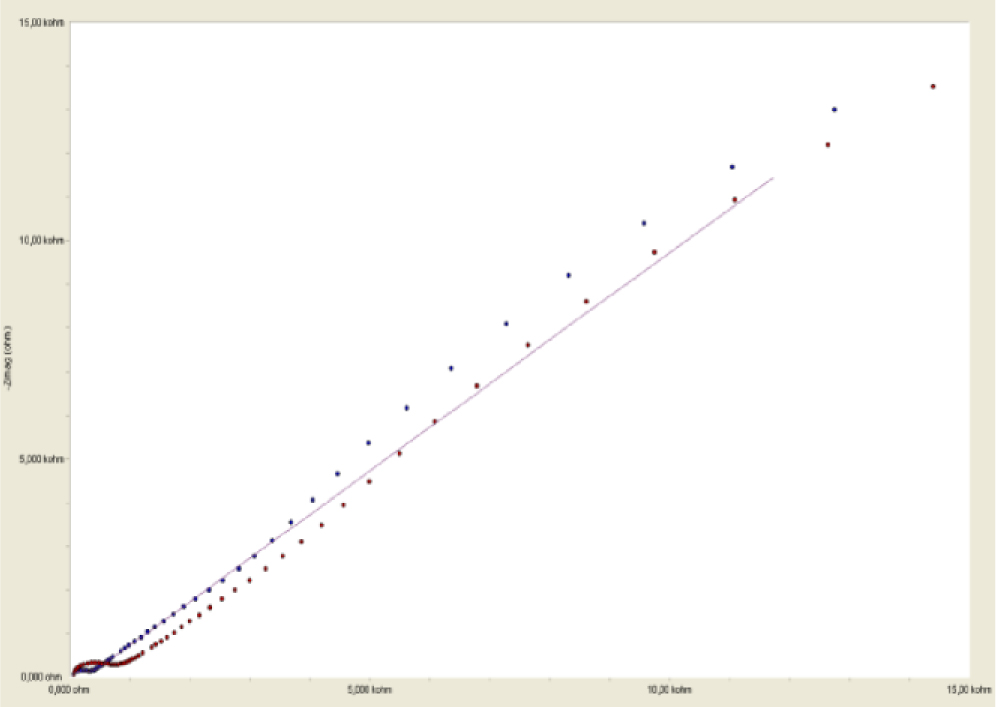
Fig. 14
Impedance Spectroscopy for cleaned and uncleaned ultrasonically welded chip
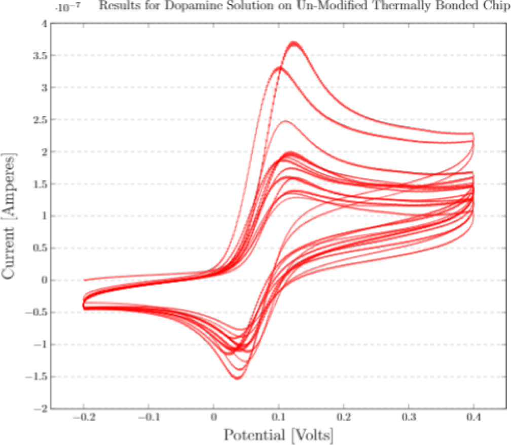
Fig. 15
CVs of dopamine detection on unmodified ultrasonically welded chip
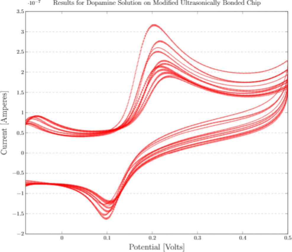
Fig. 16
CVs of dopamine detection on MPA modified ultrasonically welded chip
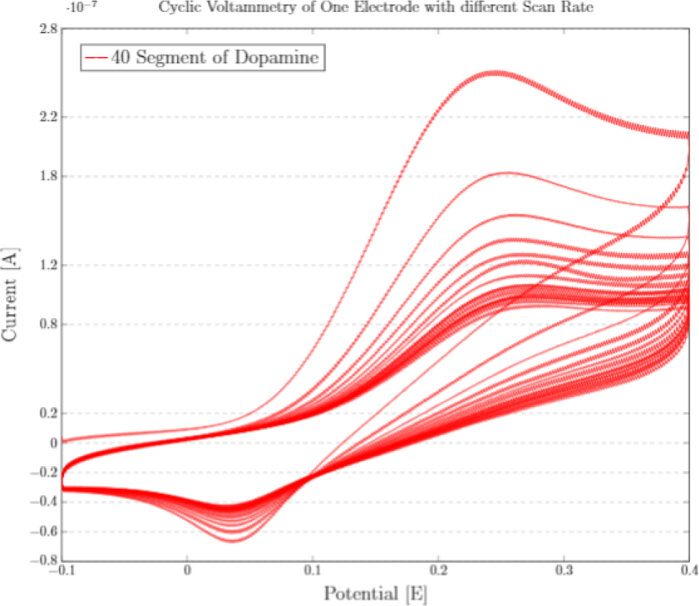
Fig. 17
CVs of dopamine detection on cysteamine. modified thermally bonded chip
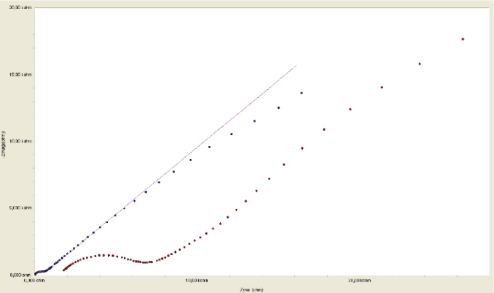
Fig. 18
Impedance spectroscopy for dopamine detection on thermally and ultrasonically bonded chip
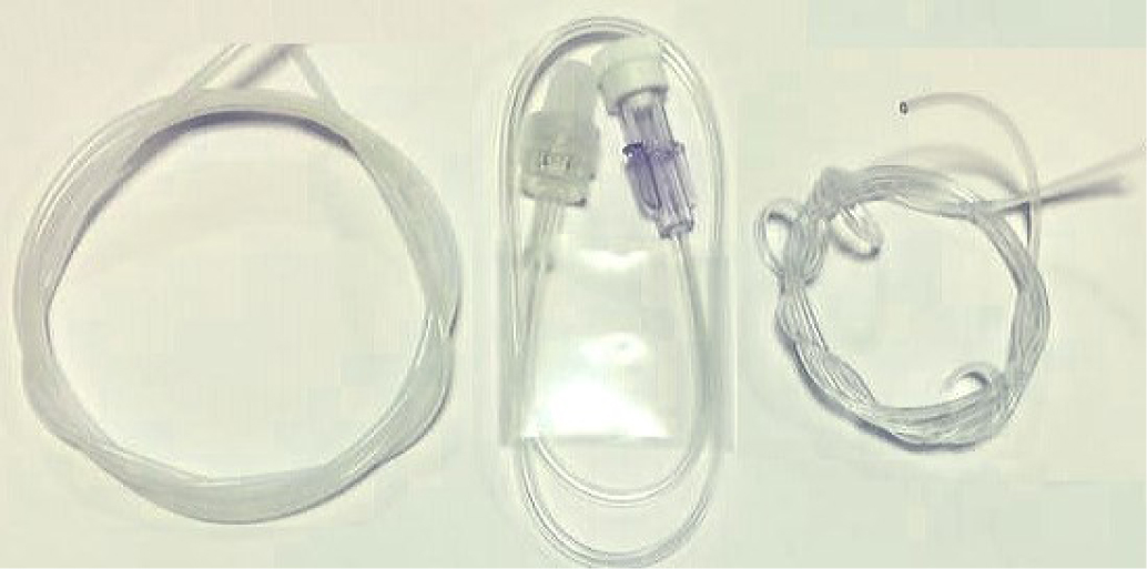
Fig. 19
Tubing with different dimensions to find the suitable dimension for the flow-injection method
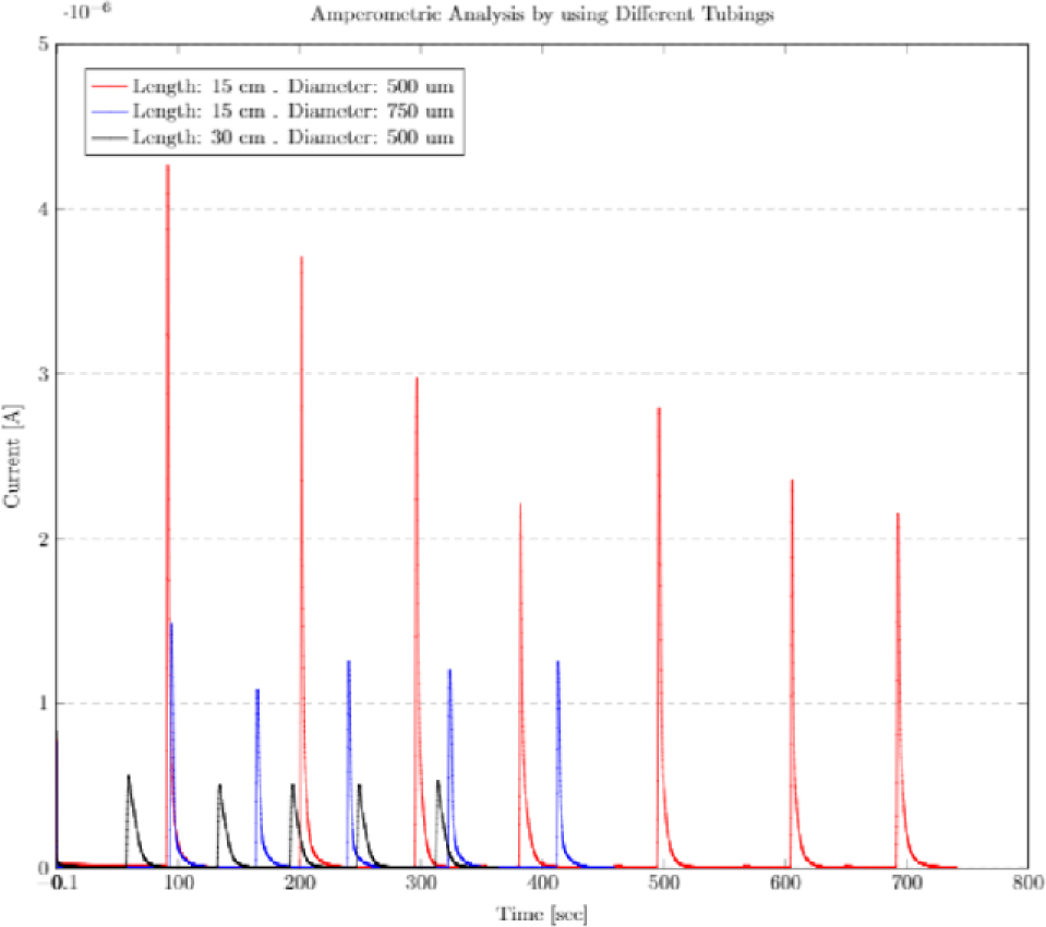
Fig. 20
Influence of different Tubings on flow injection
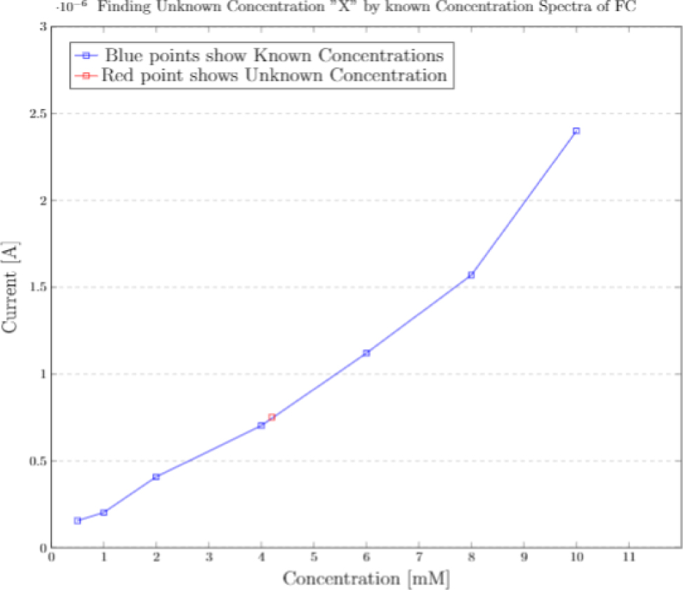
Fig. 21
Cyclic amperometry results for detection of unknown concentration of ferricyanide analyte
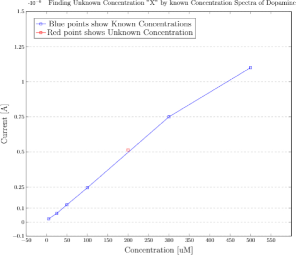
Fig. 22
Cyclic amperometry results for detection of unknown concentration of dopamine analyte