Have a personal or library account? Click to login
Double-layer microwave absorber based on nanocrystalline CoFe2O4 and CoFe2O4/PANI multi-core/shell composites Cover

Double-layer microwave absorber based on nanocrystalline CoFe2O4 and CoFe2O4/PANI multi-core/shell composites

Open Access
|Feb 2017

Figures & Tables

XRD patterns of samples S1, S2, S3 and S4.
TEM (a, b, d, f) and SEM (c, e) images of the sample S1 (a), S2 (b), S3 (c, d) and S4 (e, f).
Schematic illustration of the synthesis process of CoFe2O4/PANI multi-core/shell composites.
Hysteresis loops at room temperature for sample S2, S3 and S4.
Variation of complex permittivity and permeability of sample S2, S3 and S4 with frequency.
Sketch map of incidence of electromagnetic wave in multi-layer absorber.
Absorption curves of the layers with thickness d = 2.0 mm (a), 2.5 mm (b), and variation of dielectric loss tangent (c) and magnetic loss tangent (d) of sample S2, S3 and S4 with frequency.
Absorption curves of the double-layer absorbers with a total layer thickness d = 2.0 mm (a), 2.5 mm (b).

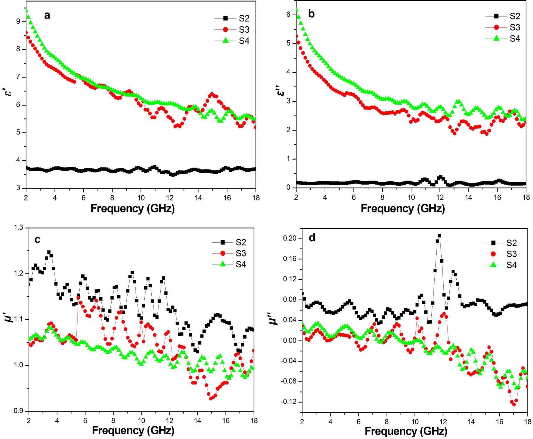
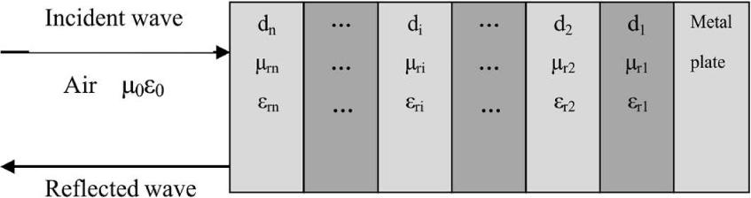
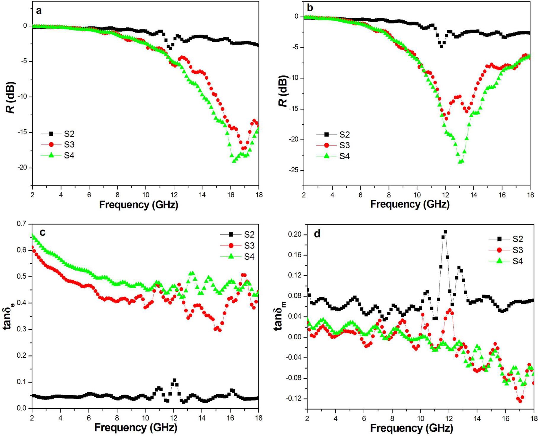
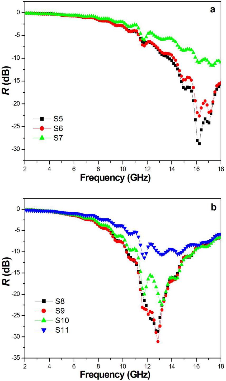
Microwave absorption properties of single layer (S2-S4) and double-layer (S5-S11) absorbers with total thickness of 2_0 mm and 2_5 mm_

SampleMaterialThickness [mm]Total thickness [mm]Min. R [dB]R peak [GHz]Bandwidth R < –10 dB [GHz]
S2Calcined ferrite2.02.0–3.211.7
2.52.5–4.811.8
S3Ferrite/PANI composite2.02.0–17.417.014.9 – 18.0 (3.1)
2.52.5–16.612.111.1 – 14.5 (3.4)
S4Ferrite/PANI composite2.02.0–19.016.214.1 – 18.0 (3.9)
2.52.5–23.613.110.8 – 14.5 (3.7)
S5Layer 1: S20.52.0–28.816.213.8 – 18.0 (4.2)
Layer 2: S41.5
S6Layer 1: S21.02.0–22.316.214.2 – 18.0 (3.8)
Layer 2: S41.0
S7Layer 1: S21.52.0–11.617.315.9 – 18.0 (2.1)
Layer 2: S40.5
S8Layer 1: S20.52.5–28.812.810.3 – 15.8 (5.5)
Layer 2: S42.0
S9Layer 1: S21.02.5–31.112.810.3 – 15.8 (5.5)
Layer 2: S41.5
S10Layer 1: S21.52.5–22.413.211.1 – 15.8 (4.7)
Layer 2: S41.0
S11Layer 1: S22.02.5–11.211.711.5 – 12.0 (0.5)
Layer 2: S40.5
DOI: https://doi.org/10.1515/msp-2017-0010 | Journal eISSN: 2083-134X | Journal ISSN: 2083-1331
Language: English
Page range: 94 - 104
Submitted on: Jan 23, 2016
Accepted on: Nov 30, 2016
Published on: Feb 24, 2017
Published by: Wroclaw University of Science and Technology
In partnership with: Paradigm Publishing Services
Publication frequency: 4 issues per year

© 2017 Yewen Xu, Guozhu Shen, Hongyan Wu, Bin Liu, Xumin Fang, Ding Zhang, Jun Zhu, published by Wroclaw University of Science and Technology
This work is licensed under the Creative Commons Attribution-NonCommercial-NoDerivatives 3.0 License.