
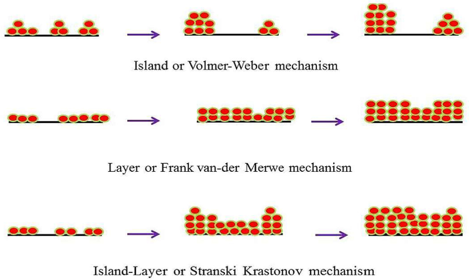
Fig. 1
Illustration of the basic nucleation modes.
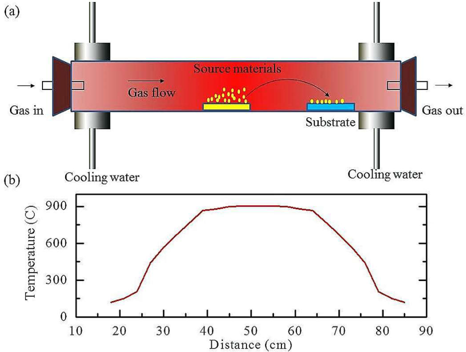
Fig. 2
(a) Schematic of the physical vapor deposition reactor, (b) temperature gradient measured inside the furnace tube.
Table 1
Summary of the growth conditions and vapor concentration in furnace tube of PVD reactor (Source temperature 900 °C, growth temperature 441 °C, source before deposition: 0.1044 g, after deposition: 0.000 g).
| Time [min] | 1 | 5 | 8 | 13 | 18 | 23 | 33 | 46 | 66 | 71 | 76 | 81 | 86 | 91 | 160 |
| Temp. [°C] | 300 | 450 | 600 | 770 | 900 | 900 | 900 | 900 | 900 | 900 | 900 | 800 | 700 | 600 | 300 |
| Pressure 0.1 Pa | 1.4 | 1.4 | 1.4 | 1.4 | 1.4 GFC** | 1.4 | 1.0 | 1.0 | 8.6 | 8.6 | 7.4 | 7.4 | 7.4 | 8.6 | 1.4 |
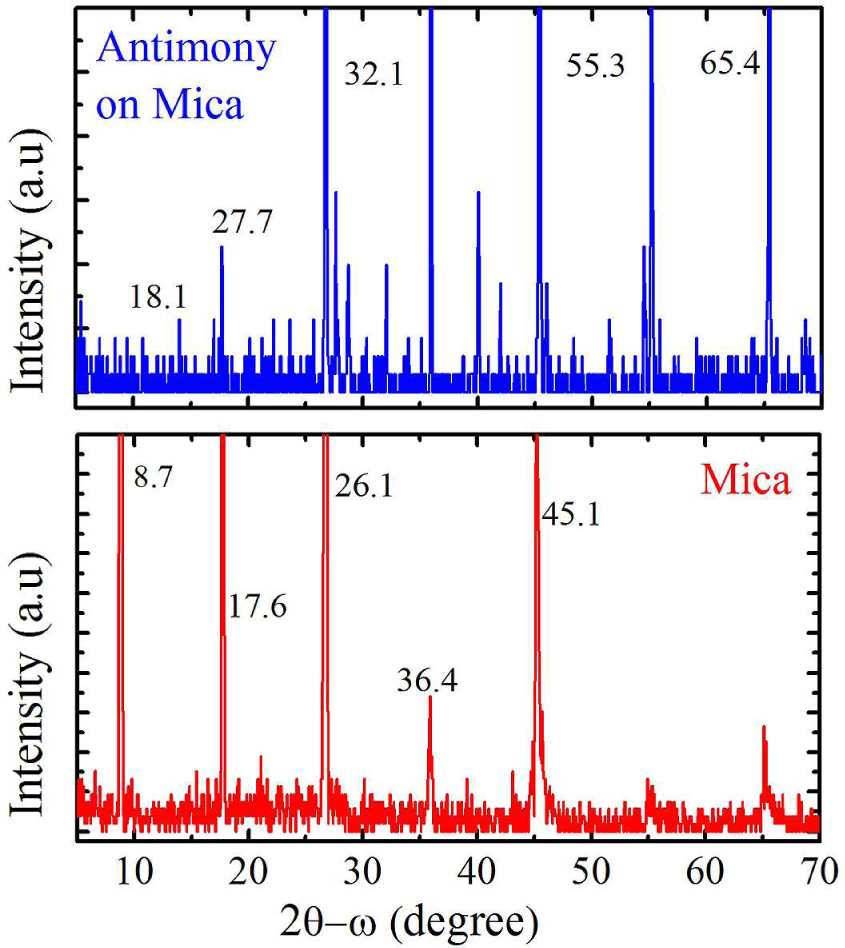
Fig. 3
XRD patterns of antimony coated and uncoated mica.
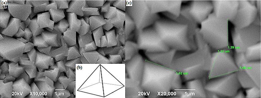
Fig. 4
SEM micrographs of the antimony thin film grown on a mica sheet.
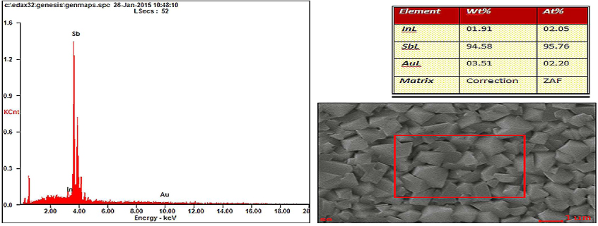
Fig. 5
Pre-annealing EDX and SEM of antimony film.
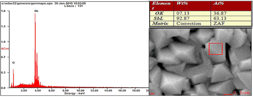
Fig. 6
Post-annealing EDX and SEM of antimony film.
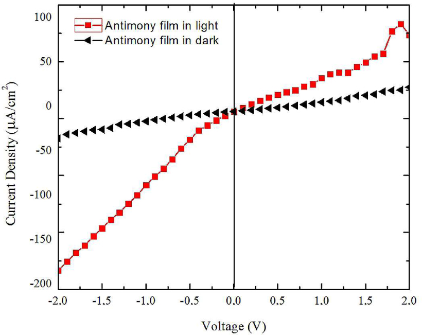
Fig. 7
Current density-voltage (j-V) characteristics of antimony thin film under dark and light scenarios.