
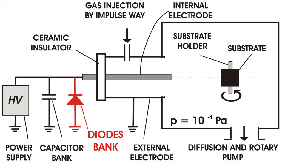
Fig. 1
Schematic diagram of the IPD device equipped with diodes bank.
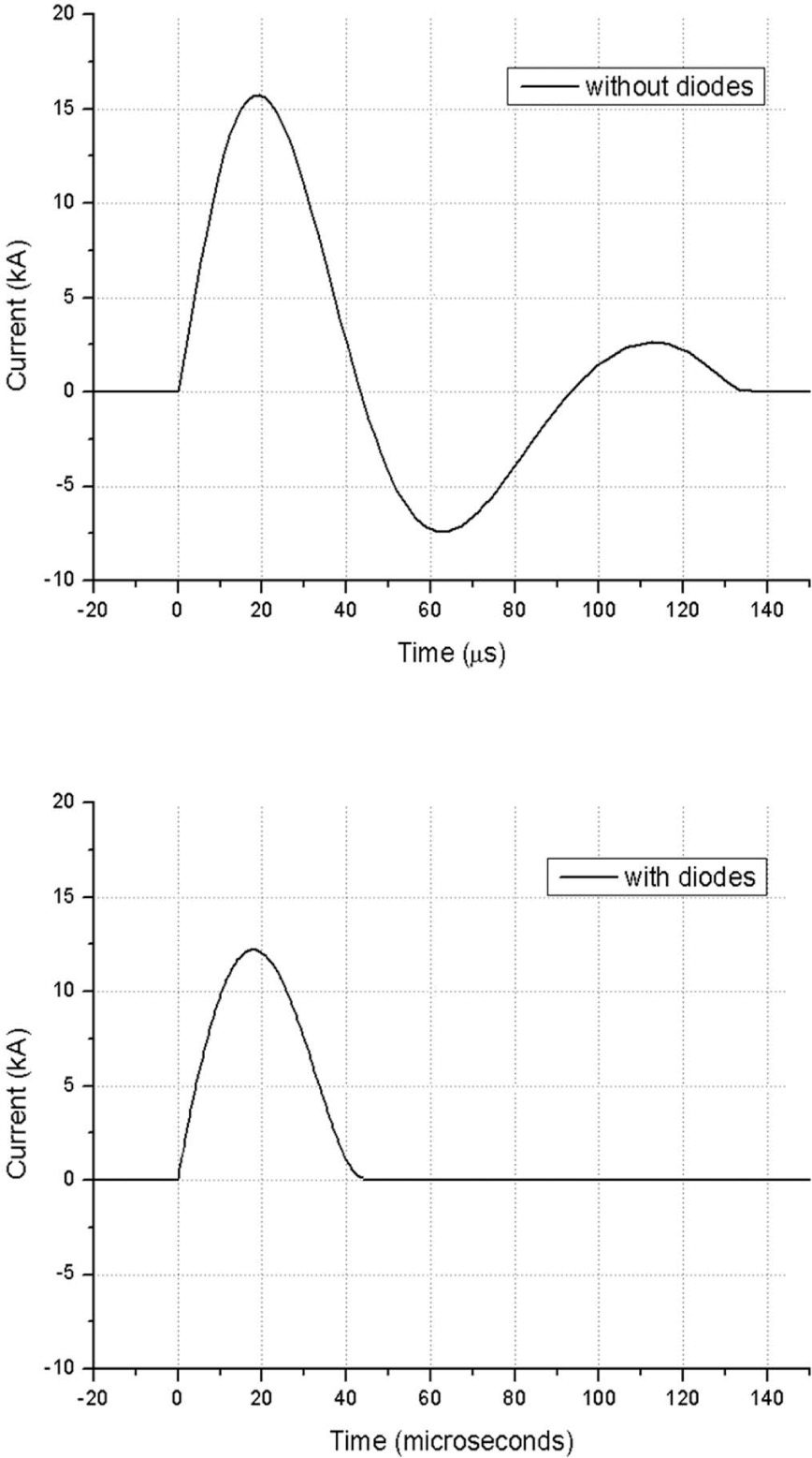
Fig. 2
Current waveforms measured in the plasma accelerator electric circuit equipped with diodes bank (lower graph) and without the diodes bank (upper graph).
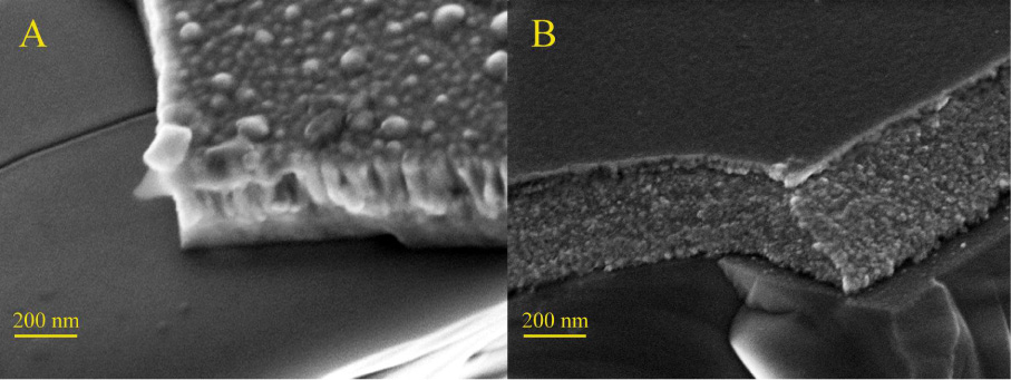
Fig. 3
SEM images presenting structures of TiN coatings deposited by processes with diodes bank connected to accelerator circuit (B) and without it (A).
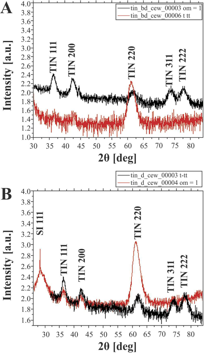
Fig. 4
X-ray diffraction patterns for the films obtained in the standard version of apparatus (A) and in apparatus equipped with diodes bank (B).
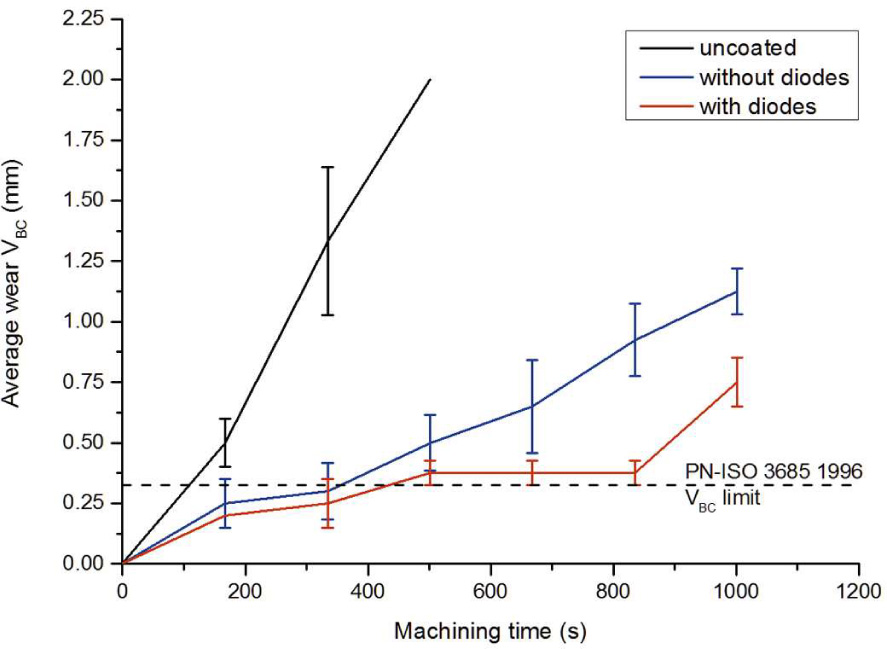
Fig. 5
The indicator of the edge blunting (VBC) as a function of machining time for three types of inserts.