
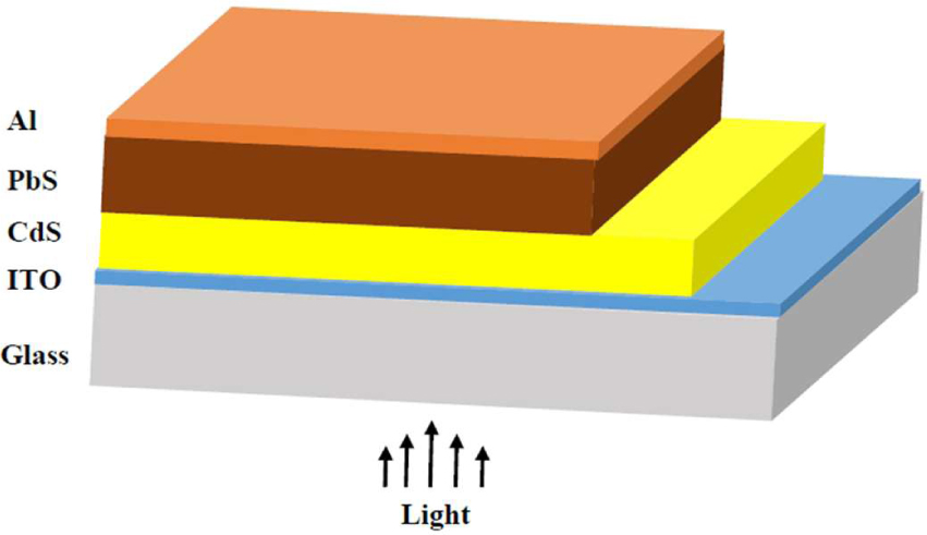
Fig. 1
Schematic diagram of a fabricated solar cell.
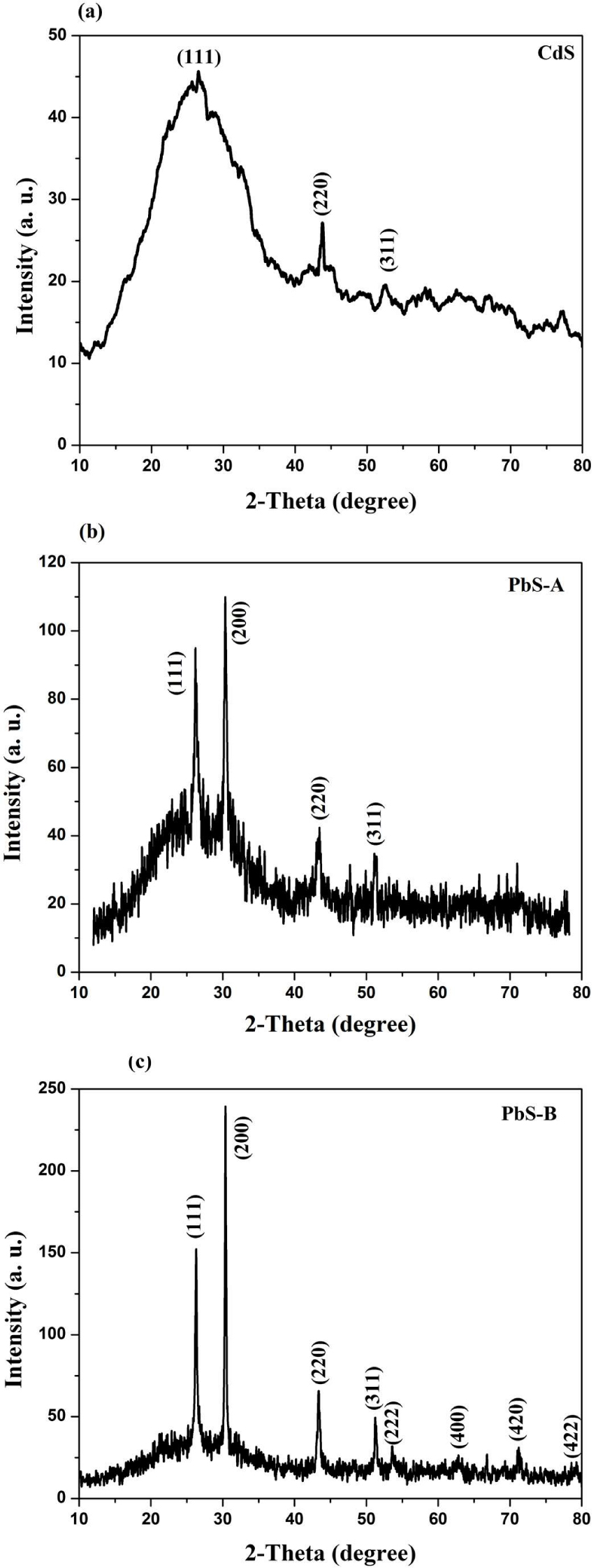
Fig. 2
XRD patterns of (a) CdS thin films and PbS films (b) with and (c) without TEA.
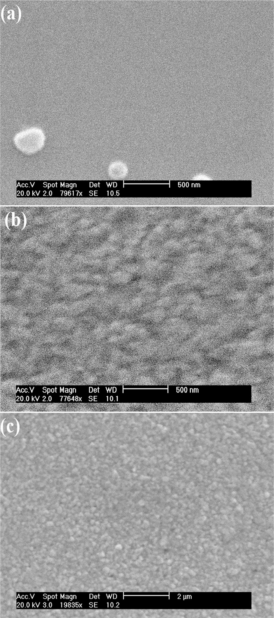
Fig. 3
SEM images of (a) CdS thin films and PbS films (b) with and (c) without TEA.
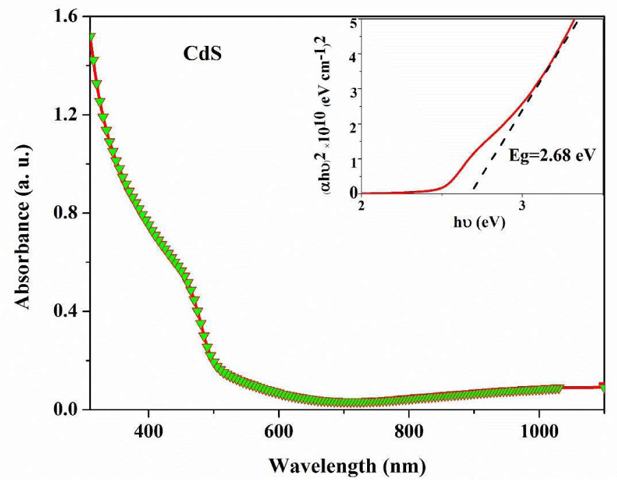
Fig. 4
The optical absorption of CdS sample at wavelengths of 300 nm to 1100 nm. The inset presents the diagram normally used to determine the band-gap of films.
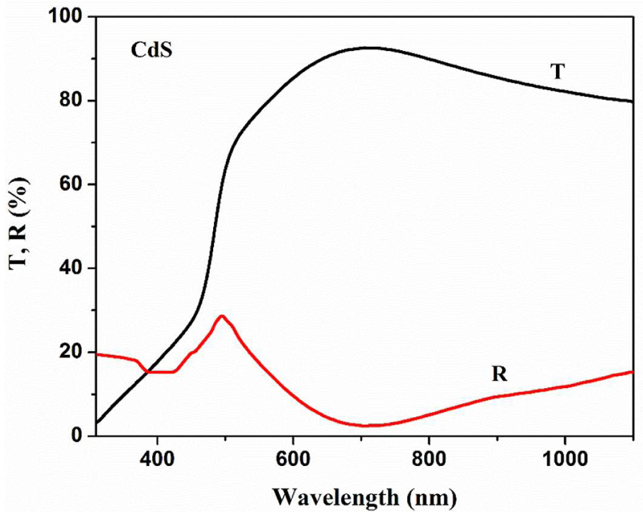
Fig. 5
The transmittance and reflectance of CdS thin film from the near-ultraviolet (300 nm) to the near-infrared (1100 nm) regions.
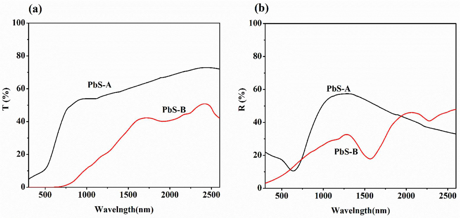
Fig. 6
The transmission and reflection spectra of PbS films with different thicknesses, 200 nm for PbS-A and 800 nm for PbS-B, deposited on glass in the spectral range of 300 nm to 2600 nm.
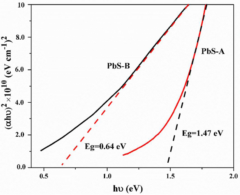
Fig. 7
Variation of (αhν)2 with photon energy for PbS thin films. The estimated band gap is about 1.47 eV for PbS-A and 0.64 eV for PbS-B.
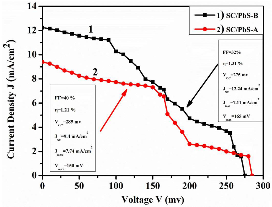
Fig. 8
The (J-V) characteristics of SCPbS-A and SCPbS-B solar cells under illumination condition of 90 mW/cm2.