
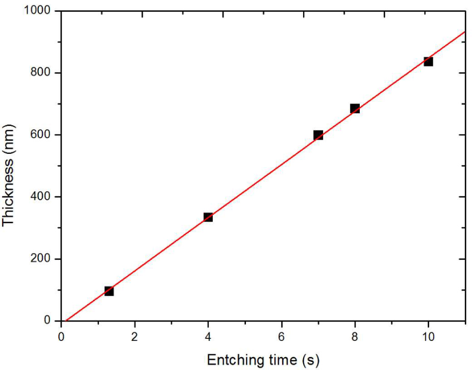
Fig 1
Thickness vs. etching time of PS grown at a constant current density of 100 mA ·cm−2 on a polished p+ substrate.
Table 1
Weighted average reflectivity calculated from the measured total reflectivity in the wavelength range between 800 and 1200 nm, for various thicknesses of PS layers.
| Weighted Thickness average R [%] | [nm] Thickness SE | [nm] SEM | |
|---|---|---|---|
| 1.3 | 52 | 96 | 79 |
| 4 | 50 | 334 | 329 |
| 7 | 48 | 599 | 560 |
| 8 | 47 | 685 | 660 |
| 10 | 44 | 836 | 836 |
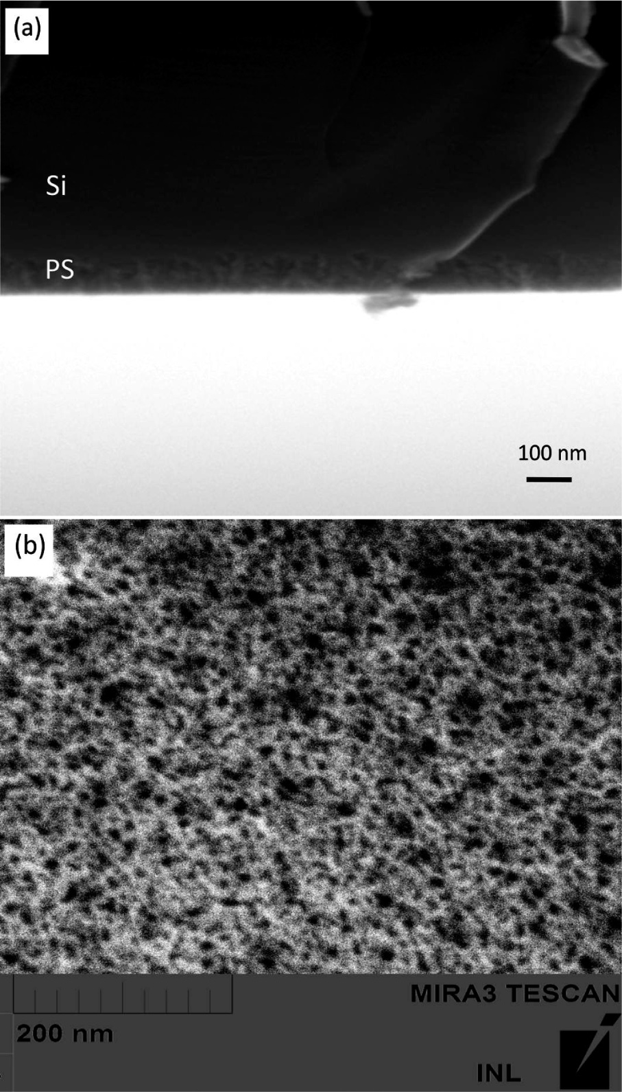
Fig 2
Cross-section SEM image of Si/PS structure obtained during 1.3 s at current density of 100 mA/cm2 on p+ substrate (a), planar view of the fabricated porous silicon layer (b).
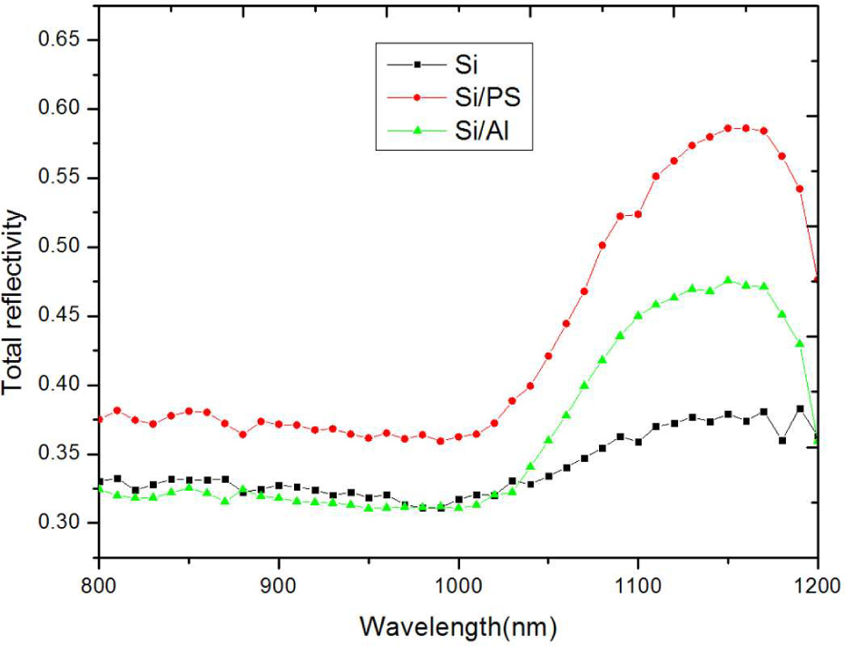
Fig 3
Experimental total reflectivity spectra for Si/PS and Si/Al.
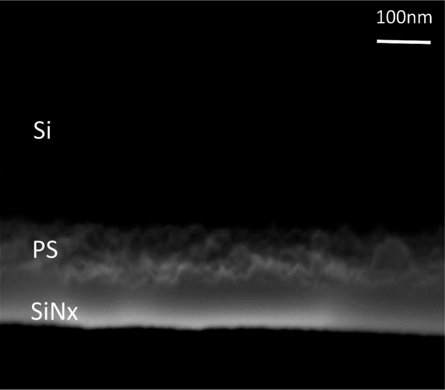
Fig 4
Cross-section SEM image of PS/SiNx structure carried out on p+ substrate.
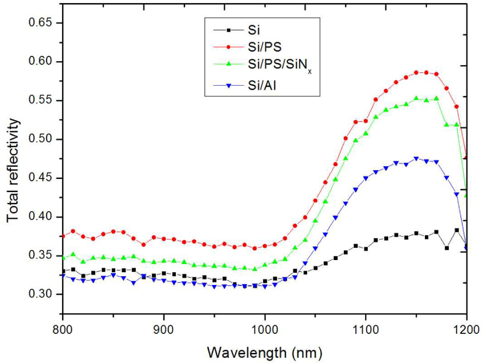
Fig 5
Experimental total reflectivity spectra for Si/PS and Si/PS/SiNx structures compared to Si/AlBSF contact.
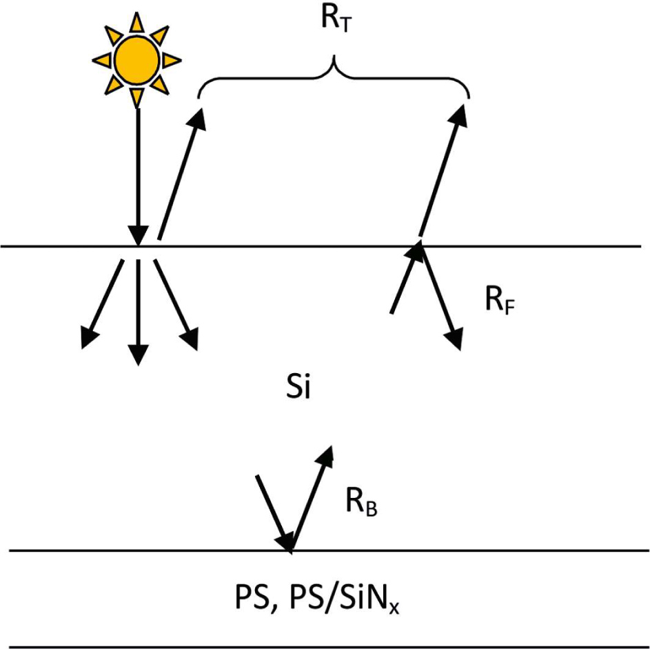
Fig 6
Optical model of a cell describing the two internal reflections (RB and RF) and the total measured reflection (RT).
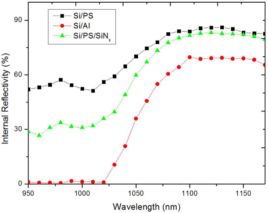
Fig 7
Internal reflectivity spectra calculated from R Tfor Si/PS, Si/PS/SiNx structures in comparison with the Si/Al reference.
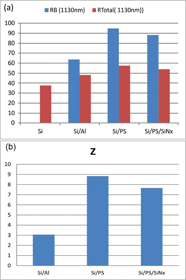
Fig 8
Total and internal reflectivity at 1130 nm (a), path-length enhancement factor (b), for Si/PS, Si/PS/SiNx and Si/Al.