
Table 1
Optical parameters of the C-Ni films deposited at different deposition times.
| Deposition | Ni | Ni nanoparticle | εbulk | εm | ωρ × 1015 | νf × 1017 |
|---|---|---|---|---|---|---|
| time [s] | [at.%] | size [nm] | [1/s] | [cm/s] | ||
| 50 | 42 | 16.44 | 0.9991 | 0.05692 | 3.11 | 4.31 |
| 90 | 48 | 16.76 | 1.1848 | 0.09144 | 4.21 | 4.26 |
| 180 | 85 | 82.21 | 24.1889 | 0.40158 | 7.26 | 10.72 |
| 600 | 56 | 17.95 | 11.0576 | 0.13541 | 5.37 | 7.32 |
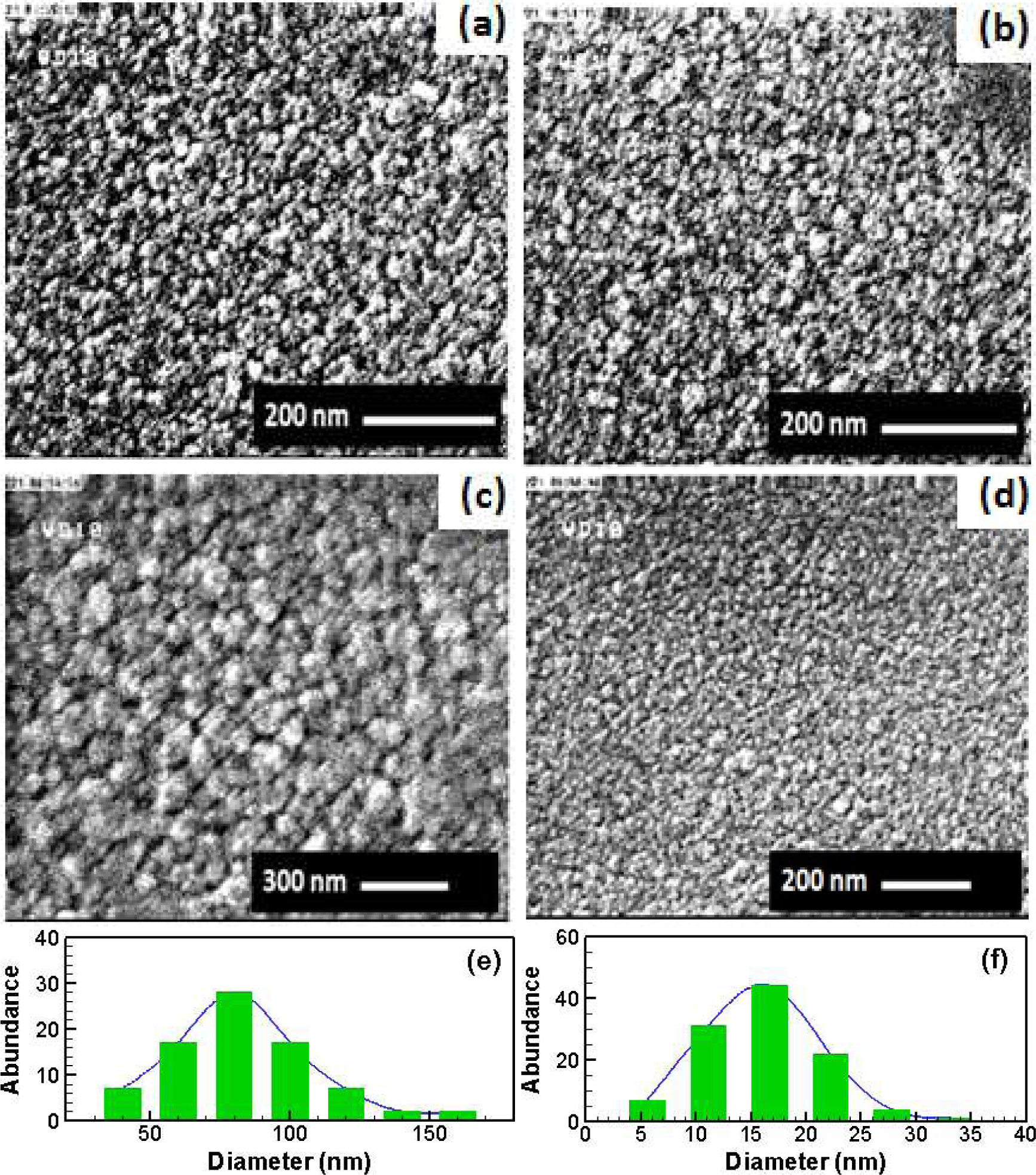
Fig. 1
FESEM images of C–Ni films deposited at deposition times of 50 s (a), 90 s (b), 180 s (c) and 600 s (d), and the size distribution of Ni nanoparticles of C–Ni films deposited at 180 s (e) and 600 s (f), respectively.
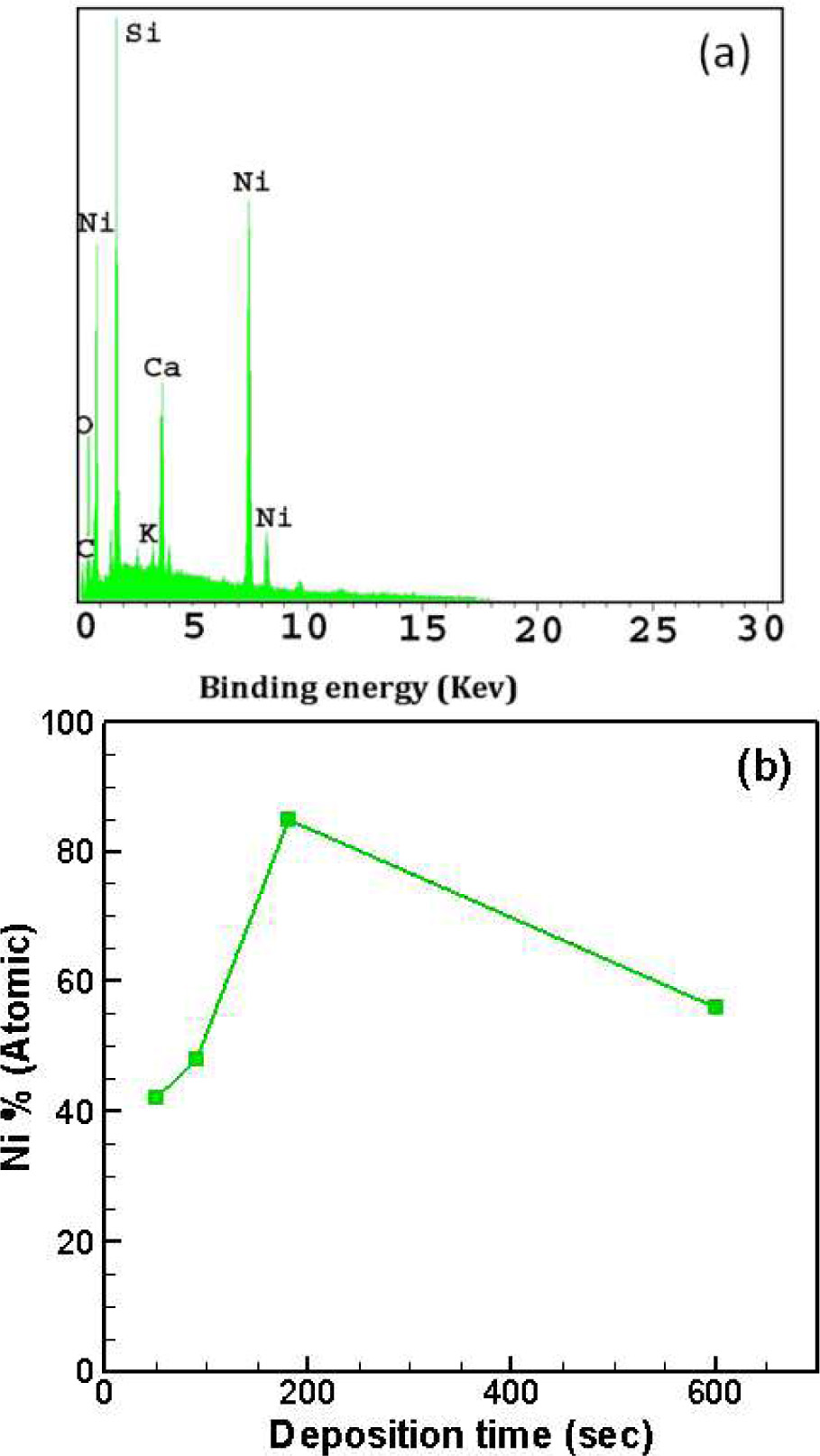
Fig. 2
EDAX spectrum of C–Ni film deposited at 600 s (a) and variation of Ni content with deposition time (b).
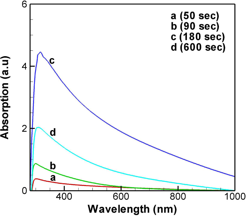
Fig. 3
The experimental absorption spectra of C–Ni films for the films deposited at different deposition times.
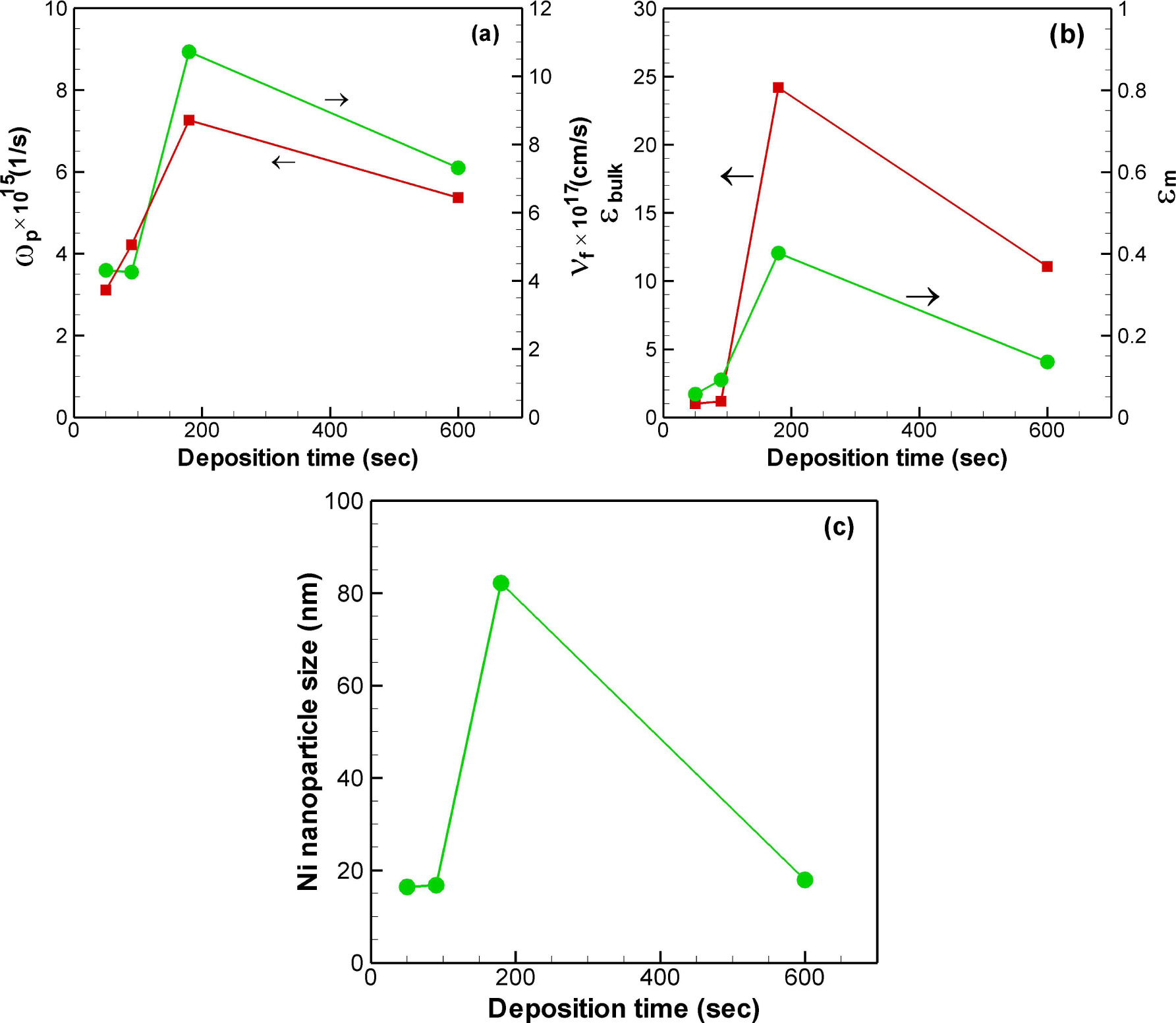
Fig. 4
Variation of ωp and νf (a), εbulk(ω) and εm, (b) and Ni nanoparticle size (c) of the C–Ni films with respect to the deposition time.
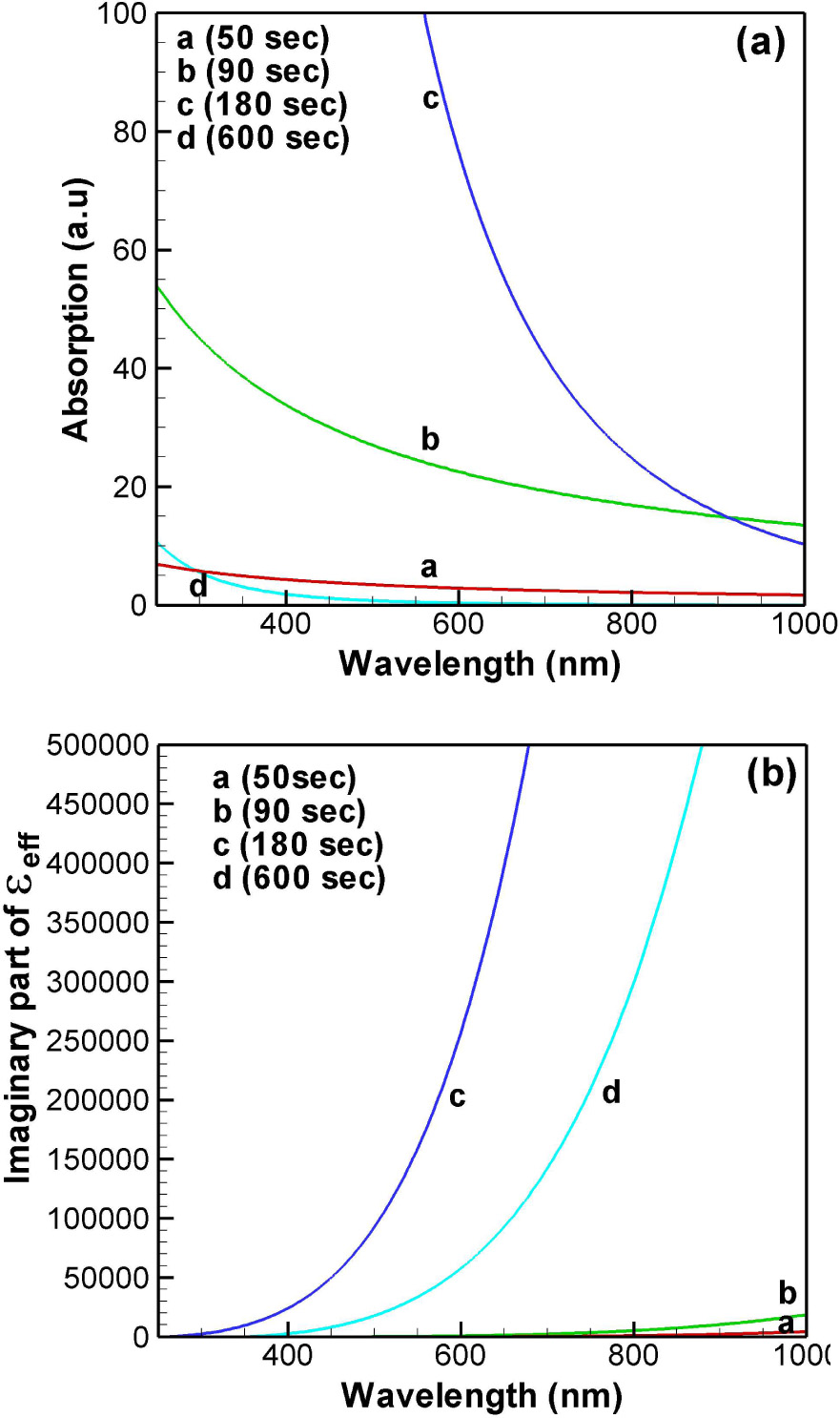
Fig. 5
The theoretical Maxwel-Garnett absorption spectra (a) and the imaginary part of the effective dielectric constant εeff (b) of C–Ni films for the films obtained at different deposition times.
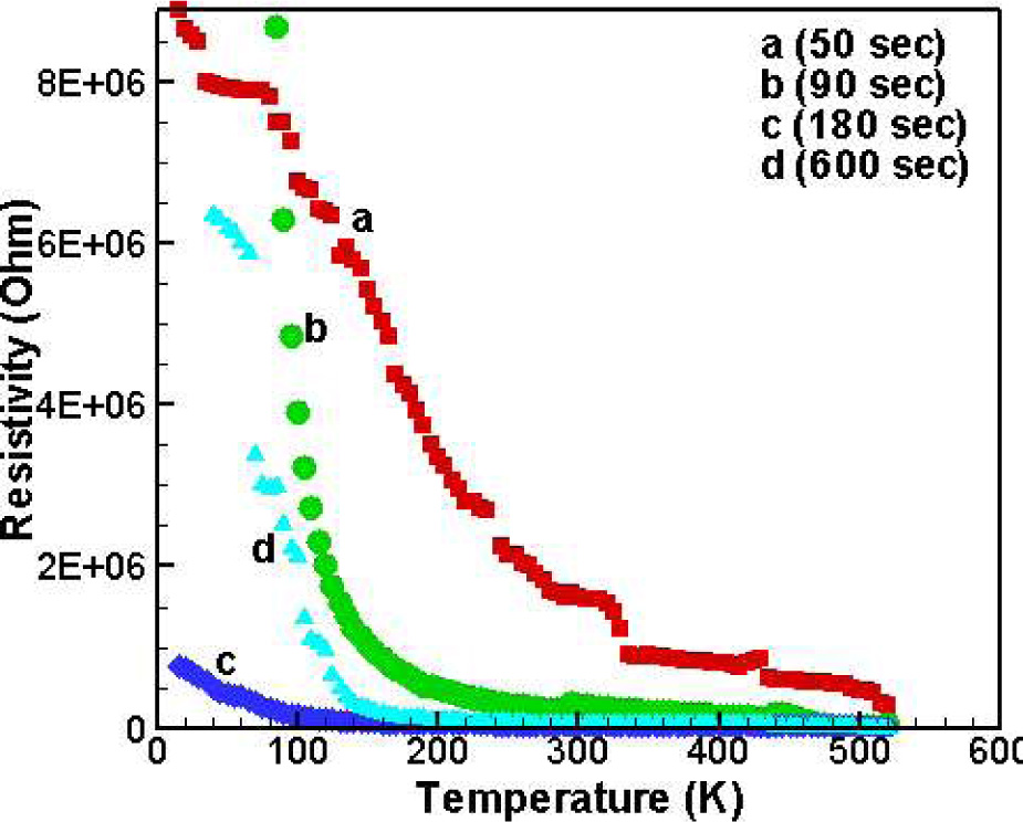
Fig. 6
Variation of resistivity with temperature for the films deposited for 50 s, 90 s, 180 s and 600 s.